

PCB history | |||||||||||
|
| 
|
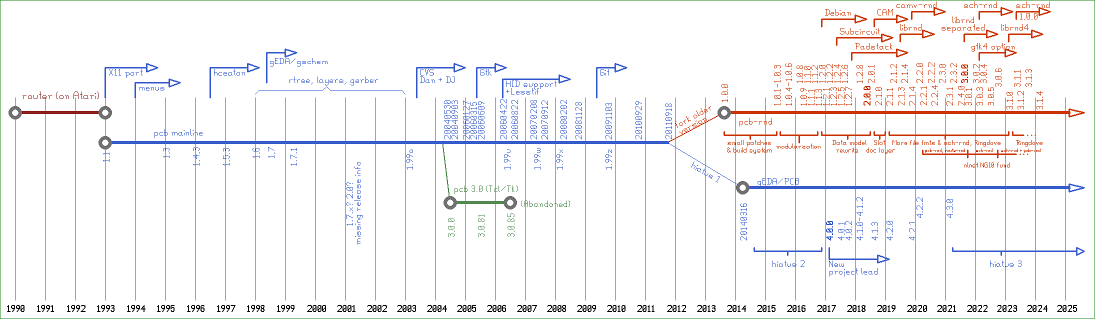
Present: from nanometers to pcb-rndThe early 21st century golden age of PCB (and probably gEDA) ended around 2011. The code got re-hosted in git. The last notable major upgrade in PCB was the nanometer conversion. Then the developer community slowly disintegrated and development stalled for years, causing a long hiatus between 2011 and 2017, with only one release in 2014. From 2017 Bert took over leading PCB, where the original PCB code is maintained. During the hiatus period, PCB was forked to pcb-rnd, in 2013. After the first few, slow steps, real intense development started in 2015. pcb-rnd got parametric footprints, modular IO that made it compatible with KiCad, eagle, autotrax and other file formats. Between 2017 and 2019 the whole data model got redesigned, which made pcb-rnd support a lot of things PCB could not (including "any layer is editable" and "any object on any layer can be added in a footprint"). All this while keeping full backward compatibility. As of 2019, pcb-rnd is where active development is happening. pcb-rnd is the project which brought the original PCB concepts from the '90s and code up to the level of a 21st century EDA. PCB is not being developed since 2021. | |||||||||

| |||||||||||
| (C) 2016..2024 Various PCB developers/maintainers and Tibor 'Igor2' Palinkas; see copying for more details. | |||||||||||