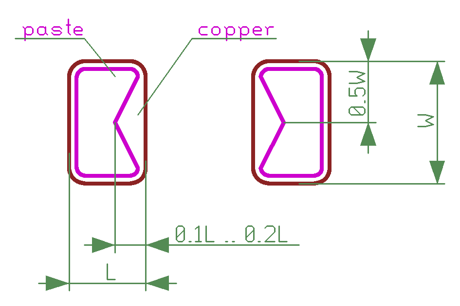
Paste size should always be without sharp corners, especially for small area pads. Rounded corners improve paste release and reduces the need of stencil cleaning between paste applications.
The area of paste (together with the thickness of the stencil sheet) determines the volume of solder paste dispensed on the pad. Too little and the solder joint will not be reliable, too much and the reflow process can produce free wandering solder beads or a smaller SMD part can produce tombstoning. IPC7525a has details on stencil design. The rule of thumb for size is:
For 2 terminal passives that are 0603 or larger it is recommended to remove some paste in the following pattern, to reduce the risk of forming solder beads during reflow (Figure 3.6).

Cylinder cap SMD like melf/minimelf requires C-shaped paste.
These should be done as polygon paste shapes in the same padstack.
There are a bunch of other shapes in use.
Bob Willis shared an excellent video demonstrating how stencil pattern avoids beading.
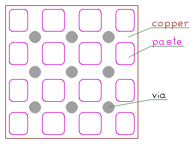
Center pads of footprints like QFN, QFP, some SOIC, etc, are often used for heat sink purpose. This requires vias to be added and such vias could easily suck in solder paste (we normally do not assume plugged/filled vias). Another problem is having too much paste on a large pad, especially in one large solid area, is higher solder dome during reflow on which the component would float causing greater distance to pcb on the signal pads. To avoid these problems a mesh pattern of smaller apertures should be used, as shown on Figure 3.7.

This shall be done using separate round corner rectangle polygons on the paste layer (and not using padstacks), while the center pad padstack itself shall not have a paste shape. Paste should avoid vias.
Total area of the paste should be between 50% and 80% of the area of center pad copper.
As a second line defense against via sucking up solder paste, it's also recommended, probably by IPC-7093A to draw the same mask pattern as the paste pattern. This way the paste+mask (over the larger copper pad) is Solder Mask Defined. The mask grid between the paste meshes would tent vias and potentially block adjacent paste areas to merge during reflow.
To avoid problems with minimum mask width, make the gap between paste meshes at least 0.3mm ( NXP recommends 0.4mm in section 4.2.2.2). The mask, fully covering vias, should extend at least 0.15mm beyond via drilled hole. For example if the via hole is 0.3mm, the mask (and no-paste) diameter over the via should be of diameter 0.6mm or larger.
According to NXP a good choice for viagrid would be 0.3mm vias on a 1.2mm pitch regular grid.
Paste pattern meshes should also have a small chamfer or rounding to avoid sharp corner and potentially easy paste release.
Example centerpad-only footprint, with 0.3mm via hole, 0.3mm mesh separation, SMD (mask+paste mesh) over a large centerpad.
In some special cases the paste shape may go over the edge of the copper pad shape. The excess paste will be sucked up by surface tension during reflow. The reason for using paste pattern slightly larger than the copper pad is typically related to stencil printing technology:
Avoid overhang unless there is a strong, documented reason to use it.