Ringdove EDA, pcb-rnd and bedrock-rnd uses the term footprint to describe the reusable graphical+metadata block that would normally host a component on a PCB. This document uses footprint in this sense and does not use the term land pattern outside of this section.
The IPC-7351 standard uses the term land pattern for the same concept and uses footprint for the surface where the component actually touches copper pads, where solder joint is made.
From fabrication point of view it is often defined as footprint being the actual physical surface where the component touches the board (so it is the geometry of the component) while land pattern is the geometry of the copper pads on the PCB. In this interpretation a land pattern is always bigger than the corresponding footprint. A single land pattern may be uses with slightly different parts (footprints). Example definitions: madpcb , a PCB HERO employee, protoexpress.
Some fabs may have slightly different interpretations: raypcb
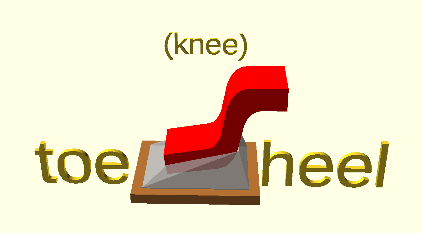
The terminology for the solder joint of an Surface Mount Device (SMD) is modeled after the anatomy of a leg, as shown on Fig. 3.1.

The two ends of the solder cone along the short edge of the pad are called toe (at lead end) and heel. The solder cone along the longer edges of the pad are called side.
In footprint design for SMD components the basis for determining the dimensions of the copper pad largely depends on the expected shape of the solder cone. Taken vertical cross sections of the above image, the solder cone is somewhat triangular with different slope angle on the toe, heel and side parts. Taking a series of horizontal cross sections of the solder cone, from top to bottom, the cross section area is constantly increasing until we reach the copper pad.
This is just a crude approximation: in reality the outer walls of the solder cone are not flat planes but curved. But for footprint design that doesn't matter much, we are interested only in the top and bottom horizontal cross sections. The top cross section's area is basically the area of the of the part's lead (pin) that would touch the PCB when placed on top of the PCB, while the bottom cross section is the area of the pad. Pad area is almost always larger than lead/pin area, to get a reliable and mechanically stable solder joint.
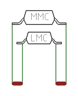
The archetypical example of having to deal with tolerances is when there are two pads (e.g. in 1206) or two rows of pads (e.g. in SOIC) in the footprint. From the component's point of view this means two rows of leads/pins. Normally the pad would be as small as the bottom side of the lead/pin touching the PCB plus some extra area for the solder cone (as described in 3.1.1). However there is a certain manufacturing tolerances, which means actual components will come in the smallest possible size (LMC, Least Material Condition) and largest possible size (MMC, Most Material Condition), from the same vendor, with the same part number. Pad dimensions should be determined so that the footprint can host both the LMC and MMC case (as shown on Figure 3.2). In other words the footprint always works for the given component within the tolerance specified by the vendor.

Furthermore there are other tolerances to consider, such as the tolerance of PCB manufacturing or the tolerance of component placement.
The naive solution to the problem would be computing the absolute worst case extremes: when the largest (or smallest) part is placed furthest away from the originally planned position on a board printed with the worst displacement of the pad possible. This would obviously result in a footprint that really always works, but at a cost of very large pads. The industry settled with a different method for accumulating tolerances: the RMS (Root Mean Square).
When a value A has a tolerance, that means there's a minimal (LMC) and a maximal
(MMC) value A can take. Tolerance of A is then:
Atol = Amax - Amin
With RMS if there are 3 different source of errors specified by tolerance,
Atol, Btol and Ctol, the final tolerance
value to use is
sqrt(Atol*Atol + Btol*Btol + Ctol*Ctol).
Implementation details are described in section 3.4.1.
Different boards may have different density goals. For example on a cell phone motherboard components need to be packed very tightly even if that means more expensive fab processes, while on cheap, throw-away consumer electronics where PCB size is not a limiting factor it's better to go for larger pads and larger footprints in general to reduce costs and risks.
In footprint design this generic density goal is indicated by 'A', 'B' or 'C'. 'A' is the least dense (consumer) board, 'C' is the tightest, most dense board. (Some parts of the industry also call this 'L', 'N' and 'M', but this document and bedrock-rnd uses the A..C convention exclusively).
A board designed for manual soldering should normally go for 'A' footprints. For reflow process 'B' or 'C' is better. Wave soldering may be close to 'A' with some more tweaking specific to the process.
Unless otherwise mentioned, this document assumes 'B' and that is the recommendation for normal high end footprints for the general audience. Rationale: for hand soldering much simpler, generic, low end footprints can be used and those won't require most of the advanced considerations of this doc (as the user won't even use the past layer for example). For wave soldering or critically dense 'C' boards the designer will have to manually deal with each and every footprint and match them up with the specific process available, well beyond the scope of this document. The following attribute/metadata key should be used:
| key | importance | value (purpose of the key) |
|---|---|---|
| density | recommended | a single letter A, B or C |
| Previous: Versioning | ToC | Next: Origin, centroid, orientation |
| License: CC-BY-SA 4.0 | (C) 2025 Tibor 'Igor2' Palinkas |