In reflow soldering using the correct pad size is very important. A pad too large can cause:
while a pad too small can cause:
Some other layers (mask, paste) are partly or fully based on the copper pad shape and dimensions.
For static file footprints copper pad sizes should be used from the datasheet's footprint drawing if it is present. In that case skip 3.4.1.
If footprint dimensions are not available, or a parametric footprint is created for a family of toleranced components, the method described in this section should be used to determine copper pad dimensions.
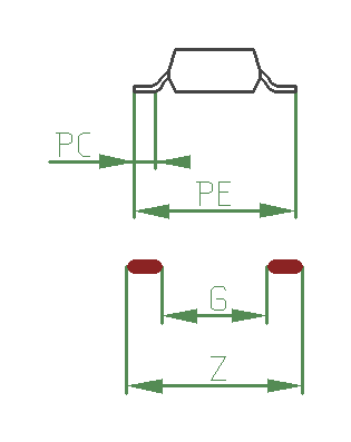
The most usual case, as mentioned in 3.1, is when there are two rows of leads/pins on opposing sides, as shown on a gull-wing package (e.g. SOIC) on Figure 3.4. below.

Input is PE and PC, which are typically specified in the datasheet as a dimension with tolerance. PE is the extent measured between ends of leads and PC is the constant length (flat part of the lead where it contacts the PCB). Expected output is Z and G, which are the extent of and gap between the pads. All dimensions are in mm and all input dimensions have tolerances. Output should be determined so that both LMC and MMC parts fit.
The minimum, maximum and tolerance values for an input, e.g. PE, is defined as:
Some datasheets specify LMC and MMC, others specify LMC and tolerance, yet others specify nominal and tol. The other two, unspecified values are always easy to calculate.
The outer extent of the copper pad is the maximum value of Z:
Zmax = PEmin + 2*JT + sqrt(PEtol*PEtol + Ftol*Ftol + Ptol*Ptol)
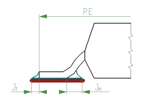
Where JT is the bottom size of the solder joint at the toe, Ftol is PCB fabrication tolerance (typically 0.1mm), Ptol is the tolerance of component placement (typically 0.05mm). The value of JT is added twice because Z is a span from end to end containing two solder joints. The value depends on lead shape and size and board density and is typically between 0.15mm and 0.8mm. The result, Z, may be rounded to the nearest 0.05mm or 0.1mm.
Gap size G is computed in a similar manner:
StolRMS = sqrt(PEtol*PEtol + 2*PCtol*PCtol)
PGmax = PEmax - 2*PCmin
Gmin = PGmax - 2*JH - sqrt(StolRMS*StolRMS + Ftol*Ftol + Ptol*Ptol)
Where JH is the bottom size of the solder joint at the heel (used twice because of the two pads included in the gap), typical values ranging from 0.15mm to 0.8mm. StolRMS is the total pad length tolerance considering the tolerances of input pin extent and input contact length. PGmax is the worst case pin gap on the component. The meaning of JH and JT are shown on Figure 3.5.

Finally a very similar computation is done on a perpendicular plane to find the height of the pad. The input for this is the width of a lead/pin, PT and the expected solder joint side size, JS, typical values ranging from 0mm to 0.3mm.
Xmax = PTmin + 2*JS + sqrt(PTtol*PTtol + Ftol*Ftol + Ptol*Ptol)
SMD pads are typically rectangular. It is preferable to have rounded corners with a radius of about 25% of the shorter edge of the rectangle but not more than 0.25mm. There are multiple reasons for the rounding:
Note: since the area lost in corner rounding wouldn't have participated much in the solder joint, the basic dimensions of the pad shall not be increased as a compensation for rounding.
The most common reason for a footprint to contain vias is center pad heat bridging (e.g. on qfn or qfp parts). In such case it is best to create a large rectangular padstack for the center pad, with no paste and another via padstack with no top side copper, paste or mask. Top side copper should be provided by the rectangular pad only. (The paste layer will need to have a mesh pattern in this setup; this is discussed later).
If vias are added for other reasons, e.g. fanout, consider placing the via away from exposed copper pads. If the via absolutely needs to be placed on the pad, paste patterns and/or via plugging needs to be considered.
The footprint shall always specify finished hole diameters, not tool diameter.
Minimum concentric copper diameter around a circular hole shall be:
Dcoppermin = Dhmax + 2 * R + T
Where (size recommendations assume density 'B') for external copper layers:
On internal copper layers R and T could be divided by 2, but R must be at least 0.1mm; use smaller internal copper only when pitch is smaller than 0.127mm.
Dhmax should be chosen to be 0.35mm larger than the maximum pin diameter and if not already round, rounded up to the next 0.1mm value. For non-circular pins diameter is measured across the diagonal.
For example a typical DIP package would have a 0.6mm max pin diameter (diagonal), which would result in an 1mm finished hole (0.95+rounding); copper pad diameter: Dcoppermin = 1.0 + 2*0.2 + 0.2 = 1.6mm
The copper ring for pin 1 shall be square (polygon shape in the padstack).
Generally the rules of 3.4.4.1 apply, but Dhmax is at least 0.5mm for plated and 1mm for unplated. Slot mechanical layer shall be drawn with round cap line in a padstack.
Some components (even SMD ones) may have plastic pins or tabs for positioning or increasing mechanical stability. The padstack of these holes must be marked unplated and the padstack shall not have any copper or paste shape but should have a mask opening larger than the hole by at least 0.1mm (so that the hole is not tented).