pcb-rnd knowledge pool
Gschem's transistor problem
| transistor_prob by Tibor 'Igor2' Palinkas on 2017-05-09 | Tags: insight, gschem, gnetlist, pin, device, mapping, footprint, heavy, symbol, pinout |
Abstract: Trouble with gschem: the transistor problem (a.k.a. heavy symbols, pin mapping, device mapping).
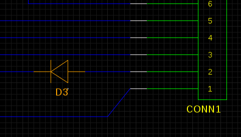
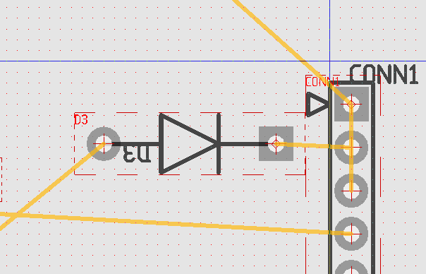
On Mon, 7 May 2018, Wed wrote:

>
I have used a parametric diode
>
alf(400.00mil,type=normal)
[and the cathod and anode are swapped].
The problem is known as the "transistor problem". It is a design error in geda/gnetlist/gschem. Unfortunately half of the developers (mainly those who never do PCBs) do not even admit the problem exists, the other half did not fix it (there are workarounds floating by). I am sorry to say, but there is a very good chance that this bug will not be fixed in that project any time soon.
Background
Everybody in the industry goes by pin numbers for majority of the components. Take the datasheet of any standard package and you will see pins are almost always numbered.
This is mainly because things do not come in custom packages, but in a few standard packages. A to220, a 8 pin DIP or a tqfp has a clear pin number assignment, regardless of what's inside the package
When you design copper of your board, you work with a package (geometry), and you want to know a pin number (which makes sense geometrically). When you take the board in your hands and want to measure something, you want to know the pin number, because you can count pins on a package but don't see if it's emitter or gpio78.
However, these are the pin numbers of the package, not the device it contains. And on the schematics side pin numbers are not too interesting and all you care about is what the pin does, the logical connection (emitter or gpio78).
So we have three concepts here; taking a NPN transistor as an example:
1. The logical concept, the transistor symbol, where you have a collector, an emitter and a base - this matters when you draw the schematics. When constructing the schematics, we rarely need to care about physical pins.
2. In the physical world however, your transistor exists as a tiny piece of die you will never see, so you need the footprint name that tells you the geometry of the large, plastic/copper/tin construct around the tiny die; this mapping is clear and mostly known by everybody who deals with PCBs. People just know what a to92 or sot23 is. The die has a model name, as it is a specific silicon construct the vendor had to design and manufacture, e.g. "bc182". Then it has a package name, e.g. sot23. So we need to know the footprint geometry (the footprint name).
3. But the manufacture also needs to wire the die to the package, e.g. connect emitter to pin 2. There is absolutely no standard as of how to do this, and even the very same device (the same subtype or model of an NPN transistor) can come with different wiring even in the same (e.g. to92) package from different vendors! At the end, when packaged, it's a bc182 or bc182-and-some-more-digits to indicate that pins are swapped, or some even stranger marking because it comes with a sot package slightly smaller than the sot23.
What goes wrong
So knowing both "bc182" and "sot23" is not enough to know the actual pinout. In other words, you need to know all three of the above.
Now the problem is, that the standard gschem->pcb process can capture 1 and 2 but lacks anything usable for 3. You place a symbol that perfectly maps the concept of an NPN transistor, then you set a footprint attribute which perfectly maps the physical package. And then you simply have nothing for also setting the pin mapping. You simply can't tell gschem that emitter is on pin 3, or "use the to92 package that contains a bc182 from my favorite vendor", unless you draw a "heavy symbol": a symbol file (1) that hardwires the package and pinout (2 and 3).
For your diode, this means you have a symbol that thinks 1=a, 2=k, while you have a footprint that thinks 1=k, 2=a. Both are perfectly fine. You will find real life examples of both assignments. They just won't work together. What you can do is an ugly workaround: use the diode-2 symbol on your schematics, which has the pin numbers in reverse compared to diode-1.
More reliable solution attempts
There was a try to overcome this problem by using symbolic names instead of pin numbers. You will find the traces of this in gschem, in pcb, and in gsch2pcb, which went on to great extents trying to rename footprint pin numbers from "1, 2, 3" to "e, b, c". It didn't work. People didn't want it. And it's because on the PCB you want to know the pin numbers, because that's what you can count.
There is the slotting mechanism too, but it is not generic enough to handle this.
And there is using heavy symbols, of course.
When I bumped into this in the late 2000s, I just wrote my own "pinmap" and "devmap" scripts. This is a 3rd solution: let gschem know about 1, let's pcb know about 3, and have an external database for 2. I'm using that ever since. But it's not part of gschem, it's just an ugly hack on top of the infra. In this setup I don't write a footprint attribute, but I write a devmap attribute in gschem. The devmap attribute is something like "2n7002_sot23", which is an external file that makes the binding between the symbol's pin _names_ and footprint pin numbers and sets the footprint attribute. This way the schematics doesn't need to know anything about pin numbers, only about the concepts, the PCB doesn't need to know anything about the concepts, only about pin numbers, and the mapping is a few liner text file that can be vendor, device and footprint specific.
The ultimate (future) solution
sch-rnd has official support for this mechanism.