pcb-rnd knowledge pool
Altium to pcb-rnd conversion
| altium by Erich S. Heinzle (VK5HSE) on 2017-02-01 | Tags: howto, file format, format, altium, convert |
Abstract: Howto convert altium boards using an external tool and pcb-rnd
Open sourced component libraries and hardware designs represent a shared, global, intellectual commons that should ideally remain freely available to educators, hardware hackers and tinkerers wherever they may be, regardless of their financial means.
Older designs developed with proprietary tools always remain vulnerable to possible changes in file formats or licensing at some point in the future.
Accordingly, designers are often keen to export their electronic designs to FLOSS EDA tool suites, such as the pcb-rnd, KiCad, or the gEDA toolsuite, but might not know how to go about it.
There is an amazing script called altium2kicad, written by thesourcerer8, and available at https://github.com/thesourcerer8/altium2kicad/
The script can convert Altium schematics and layouts to KiCad format, allowing old or legacy open hardware designs to be transitioned to FLOSS EDA toolsuites such as KiCad and pcb-rnd, preserving the designs for future users and tinkerers.
pcb-rnd is able to import and export KiCad s-expression layouts, allowing it to use the converted layouts generated by altium2kicad.
pcb-rnd can also export selected footprints in a layout as a KiCad .mod file.
Accordingly, this is a brief HOWTO on converting Altium layouts to pcb-rnd (and gEDA compatible) layouts, using pcb-rnd .
1) install altium2kicad, available at
https://github.com/thesourcerer8/altium2kicad/
2) unpack your altium design (.PcbDoc) file using
unpack.pl
3) modify convertpcb.pl around lines 1256-1260 in the perl script so that the negative Y offset is turned off (The offset allows the layout to be overlaid on matching gerbers, apparently).
4) then run
convertpcb.pl
5) strip out the comments in the converted file (example.kicad_pcb), i.e.
cat example.kicad_pcb | grep -v "#" > exampleStripped.kicad_pcb
6) load the layout in pcb-rnd , available via svn. See
http://repo.hu/projects/pcb-rnd/ It will build on OSX, and most Un*x operating systems without difficulty, and supports CLI, lesstif and gtk user interfaces at the time of writing.
The debian/ubuntu packages of pcb-rnd at the time of writing lack the modifications necessary to parse the generated layout, but the next release should contain them.
Once the layout is loaded in pcb-rnd, it can be saved using the native pcb-rnd lihata board format, or as gEDA PCB format, or as KiCad s-expression format or as KiCad legacy format.
Current limitations of the altium2kicad script are that footprints are not embedded in the layout, but the key objective of lossless conversion of the copper layers, silks screen layers and outline is essentially achieved with the script.
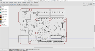
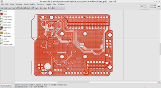
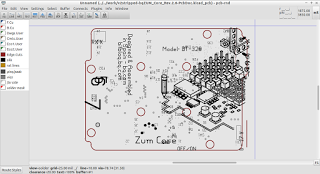
Here are some screenshots from an open hardware arduino shield, the zum board, the design files for which are available at https://github.com/bq/zum/tree/master/zum-core/PCB
after going through the above process, and then loading into pcb-rnd
And here is the same board, loaded into KiCad's pcbnew
In closing, it should be mentioned that there are other tools enabling conversion of BXL, Eagle and KiCad libraries to gEDA gschem/PCB format, and that KiCad allows gEDA footprints (but not layouts) to be imported.
Together, the FLOSS tools pcb-rnd, and KiCad, now have the ability to effectively pool and share PCB layouts and footprint designs. Happily this means that efforts can be shared and users do not need to make an either/or decision when it comes to choosing their preferred FLOSS EDA toolsuite.


