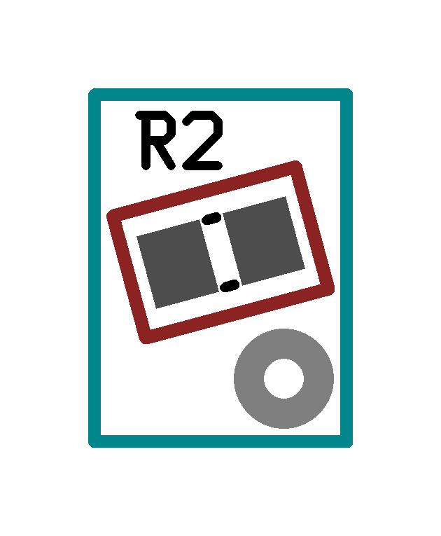
Focus is describing the metadata and block references for building a full Printed Circuit Board. The board block doesn't specify much geometry in itself but references other blocks within the same file. Thus for a full board description, a tEDAx file needs to contain several blocks, from which at least one is a board block.
Note: the order of blocks within the file is arbitrary. It is preferred to keep only one board block in a tEDAx file.
| command | parameter names | explanation |
|---|---|---|
| description | text | optional board description |
| drawing_area | x1 y1 x2 y2 | optional drawing area specification - objects shall not extend beyond the drawing area |
| attr | key value | optional key=value attributes; interpretation is up to the PCB software producing or reading the file |
| stackup | blockID | mandatory reference to a board stackup block stored in the same file; only one instance permitted |
| netlist | blockID | optional reference to a netlist block stored in the same file; only one instance permitted |
| drc | drcID | optional reference to a drc block stored in the same file; only one instance permitted |
| etest | blockID | optional reference to an etest block stored in the same file; only one instance permitted |
| place | compID blockID ox oy rot swapside role | place a footprint as a global (non-layer) object. compID is an unique
ID within the board block that will be used for referencing this
placement (typically the "refdes"; same component id as used in the
netlist); blockID is a reference to a footprint block.
Coords ox and oy are used as an offset to the placement then rotation is applied around the origin of the placed footprint. The rotation is given in angles, as a real number. Rotation takes place around the footprint origin where it is placed on the board. If swapside is "0", the footprint is instantiated with its primary side being the the top side of the board. If it is "1", it is mirrored over the x axis and placed on the bottom side. The order of transformations is: offset, rotate, mirror. role is one of comp, via or misc. Value comp means the footprint is placed for a component. In case of via, the footprint must contain at most one object per copper and mask layer and at most one hole. Value misc is for arbitrary non-comp, non-via grouping - the import code may split up the footprint into layer objects. |
| place_text | compID layerID x1 y1 x2 y2 relsize rot textstring | text object which is part of the placement of compID. The layerID must be a top or bottom silk layer. If bottom, the text is automatically mirrored. The text object is specified the same way as in layer blocks, except there's no clearance hint as this text object must be on a silk layer. |
| place_attr | compID key val | assign a key=value attribute to a placed component. The interpretation of key and value are up to the software. |
| place_fattr | compID key val | assign a key=value fixed attribute to a placed component. The interpretation of key and value are as specified in the back annotation block for components. |
Support for block references to stackup, layer and place. Place should support any angle rotation - if the CAD's internal data model doesn't support that, the tEDAx import layer should generate a new, rotated footprint and place that.
At least one place_text must be supported per component, for placing the refdes.
All place_fattrs need to be understood (worst case stored as a plain attribute).
Below is an example board that features a 0805 part rotated 15 degrees CCW. The placement text (refdes) is not rotated. There is a rectangle drawn on top copper around the part (aligned with the 15 degree rotation), a round via down right, and an axis aligned rectangular board outline on the unplated mech layer.

tEDAx v1

begin drc v1 board_drc
 rule all copper gap 0.3048 pcb_rnd_old_drc_from_conf
 rule all copper overlap 0.4826 pcb_rnd_old_drc_from_conf
 rule all copper min_size 0.254 pcb_rnd_old_drc_from_conf
 rule all silk min_size 0.1778 pcb_rnd_old_drc_from_conf
 rule all mech min_size 0.381 pcb_rnd_old_drc_from_conf
end drc

begin netlist v1 board_netlist
 value R2 0805
 footprint R2 Standard\ SMT\ resistor,\ capacitor\ etc
end netlist


begin footprint v1 sc_glob_249
 line primary silk - -0.0998 -0.6998 0.0998 -0.6998 0.2032 0.0000
 line primary silk - -0.0998 0.6998 0.0998 0.6998 0.2032 0.0000
 term 1 1 - 1
 polygon primary copper 1 0.254 4 -0.249936 -0.749808 -1.549908 -0.749808 -1.549908 0.749808 -0.249936 0.749808
 polygon primary mask 1 0.254 4 -0.173736 -0.826008 -1.626108 -0.826008 -1.626108 0.826008 -0.173736 0.826008
 polygon primary paste 1 0.254 4 -0.249936 -0.749808 -1.549908 -0.749808 -1.549908 0.749808 -0.249936 0.749808
 term 2 2 - 2
 polygon primary copper 2 0.254 4 1.549908 -0.749808 0.249936 -0.749808 0.249936 0.749808 1.549908 0.749808
 polygon primary mask 2 0.254 4 1.626108 -0.826008 0.173736 -0.826008 0.173736 0.826008 1.626108 0.826008
 polygon primary paste 2 0.254 4 1.549908 -0.749808 0.249936 -0.749808 0.249936 0.749808 1.549908 0.749808
end footprint

begin stackup v1 board_stackup
 layer top_paste top paste
  lprop top_paste display-color #cd00cd
 layer top_silk top silk
  lprop top_silk display-color #000000
 layer top_mask top mask
  lprop top_mask display-color #ff0000
 layer top_copper top copper
  lprop top_copper display-color #8b2323
 layer grp_4 inner insulator
 layer global_outline all umech
  lprop global_outline display-color #00868b
 layer bottom_copper bottom copper
  lprop bottom_copper display-color #3a5fcd
 layer bottom_mask bottom mask
  lprop bottom_mask display-color #ff0000
 layer bottom_silk bottom silk
  lprop bottom_silk display-color #000000
 layer bottom_paste bottom paste
  lprop bottom_paste display-color #cd00cd
end stackup

begin layer v1 top_paste
end layer

begin layer v1 top_silk
end layer

begin layer v1 top_mask
end layer

begin layer v1 top_copper
 line 2.276211 4.346324 2.933611 6.799776 0.254 0.0
 line 2.933611 6.799776 6.613789 5.813676 0.254 0.0
 line 6.613789 5.813676 5.956389 3.360224 0.254 0.0
 line 5.956389 3.360224 2.276211 4.346324 0.254 0.0
end layer

begin layer v1 grp_4
end layer

begin layer v1 global_outline
 line 1.905 1.905 1.905 8.89 0.254 0.0
 line 1.905 8.89 6.985 8.89 0.254 0.0
 line 6.985 1.905 6.985 8.89 0.254 0.0
 line 6.985 1.905 1.905 1.905 0.254 0.0
end layer

begin layer v1 bottom_copper
end layer

begin layer v1 bottom_mask
end layer

begin layer v1 bottom_silk
end layer

begin layer v1 bottom_paste
end layer


begin footprint v1 ps_glob_0
 hole - 0.0000 0.0000 0.8001 -
 fillcircle primary copper - 0.0000 0.0000 1.0000 0.5080
 fillcircle secondary copper - 0.0000 0.0000 1.0000 0.5080
 fillcircle inner copper - 0.0000 0.0000 1.0000 0.5080
end footprint

begin board v1 -
 drawing_area 0 0 8.89 10.795
 attr PCB::grid::unit mil
 stackup board_stackup
 netlist board_netlist
 drc board_drc
 place 218 ps_glob_0 5.715 7.62 0.000000 0 via
 place R2 sc_glob_249 4.445 5.08 15.000000 0 comp
 place_text R2 top_silk 2.680681 2.187792 4.509483 3.457793 100 0.000000 R2
 place_fattr R2 value 0805
 place_fattr R2 footprint Standard\ SMT\ resistor,\ capacitor\ etc
 place_attr R2 refdes R2
end board