Sometimes there are a set of connections which contain pin pairs that could be swapped. For example the data lines of an external parallel SRAM interface to an MCU: it doesn't matter if data bit 1 at the MCU is wired to data bit 1 or 5 of the SRAM, as there is an 1:1 mapping and no one else is using the same bus wires. In this case connections should be swapped during pcb routing and annotated back to gschem so that the schematics can be updated. Both paths are illustrated below.
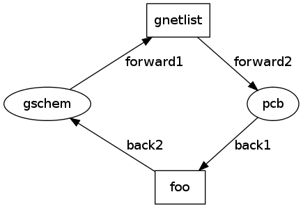
Forward annotation passes on complete netlists along arrows forward1 and forward2. Back annotation would pass back netlists, changes or modification requests on the back1, back2 path. Gnetlist takes sch files to extract and build a netlist in whatever format the receiver needs. There should be a glue layer, called foo on the drawing, that does the reverse: receives whatever format the sender has and generates something that gschem will understand.
An alternative is to keep the netlist as-is, and maintain a separate list of changes. The form proposed hereby is a table of "operation,pinID,net" or "operation,args...". Netlist operation is one of "del_conn", "add_conn" and "net_info". The table is called the netlist patch.
For example assume two components with pins A1, A2 and B1, B2, with connections n1=A1-B1 and n2=A2-B2. While routing the designer decides changing them to n1=A1-B2 and n2=A2-B1 would be easier and is acceptable by the design. The table of changes would contain this:
| op | pinID | net |
|---|---|---|
| del_conn | B1 | n1 |
| del_conn | B2 | n2 |
| add_conn | B2 | n1 |
| add_conn | B1 | n2 |
Pcb-rnd would store this table in memory. When some code calls the netlist code to find out the members of a net, or which net a given pin is connected to, after running the original netlist code, the result would be adjusted by the table.
The table would be normalized after operations. For example:
| op | pinID | net |
|---|---|---|
| del_conn | B1 | n1 |
| add_conn | B1 | n2 |
| add_conn | B1 | n3 |
| del_conn | B1 | n2 |
| op | pinID | net |
|---|---|---|
| del_conn | B1 | n1 |
| add_conn | B1 | n3 |
Pcb-rnd would save the normalized table in the pcb file in a new section. Upon a netlist change in pcb (import/load netlist or load the pcb), pcb-rnd would check each row of the table: it is easy to decide whether that row has been implemented in the netlist or not. Obsolete rows of the table would be deleted.
A corner case is when B1 is removed from n1 and then added to n2 by the table, while a new forward annotation removes B1 from n1 and adds it to n3. In this case the first row of the table is deleted, as B1 is already removed from n1, but pcb-rnd has no chance to decide if netlist adding B1 to n3 should affect the table adding B1 to n2, so that rule is kept.
net_info is used to describe the original members of a net, in the state they were before any change on the netlist occurred.
There should be a separate dialog box or a separate region of the netlist box showing the netlist patch with edit capabilities.
Finally, the most important feature would be new actions resolving shorts. Using the above example (n1=A1-B1 and n2=A2-B2 changed to n1=A1-B2 and n2=A2-B1), I believe the user would:
| action | screenshot | patch list after the actions |
|---|---|---|
|  | (empty) |
|  | (empty) |
| 
| (empty) |
| 
|
net_info n1 A1 B1 net_info n2 A2 B2 del_conn B1 n1 add_conn B1 n2 |
| 
|
net_info n1 A1 B1 net_info n2 A2 B2 del_conn B1 n1 add_conn B1 n2 del_conn B2 n2 |
| 
| |
| 
|
net_info n1 A1 B1 net_info n2 A2 B2 del_conn B1 n1 add_conn B1 n2 del_conn B2 n2 add_conn B2 n1 |
An alternative is drag&drop ratline endpoint onto snap points; it may be tricky to convert that to net/pin relations if a rat line is between two line segments, tho.
These changes would live immediately, leaving the board free of shorts and rats. There should be, however, some warning in the "congratulation" message that tells the user a back annotation is still required.
There are multiple ways pins can be connected to a net in gschem. It's probably not a good idea to have too much automatism in the gschem's side, trying to actually removing connections and adding new ones using the patch (or whatever info foo converted the patch into).
However, gschem should support four things natively:
Displaying unwanted connections happen at:
TODO: there are a lot to think over about special cases related to multipage schematics, hierarchies, slots, split symbols.
There are other parameters that sometimes change during routing. A common case for my 1 or 2 layer boards is when I originally intend to use 0603 parts but during routing I figure I need to pass a trace between the pads. I need to change the part to 0805 or 1206 (for two traces). I'd like to be able to do this in-place in pcb with an action that replaces the footprint but keeps the origin in place. This obviously still requires some manual fiddling afterwards, but would remove the long, tedious chain I have now:
The new process would be:
The same thing could work for values, which is the other attribute PCB also
sees. The same mechanism could work from other programs as well, e.g. tuning
the values of some parts in a simulator and then back annotating the changes
to the schematics. The patch table format foo handles would be in the
simplest plain text form.
(or it could be a del_attrib and add_attrib pair, like with connections)
Amendment 2: examples from gschem's point of view (3rd Sep)
netlist change
del_conn netname1 U1-1
add_conn netname2 U1-1
attribute change: footprint change
change_attrib U1 footprint=DIP(8) footprint=SO(8)