Convention: typedef'd types are called pcb_*_t - the corresponding struct is pcb_*_s.
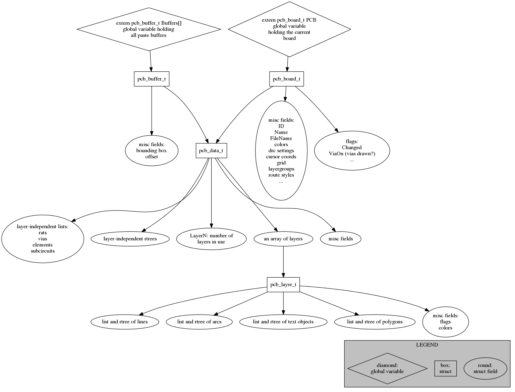
There is only one board being edited. A board is the model of the whole world for pcb-rnd - any other, auxiliary data is only a partial description of a board. The data struct for board is pcb_board_t. As of now, pcb-rnd edits only one board at a time, and it is stored in a global variable called PCB. The code is single threaded and is not reentrant.
Half of the board structure describes global board properties:
Relevant structs, variables and functions are in board.[ch].
A pcb_data_t contains everything to describe the 2d geometry of an existing board:
Relevant structs, variables and functions are in data.[ch].
However, it does not contain the layer stackup, but references to it. This means a data_t can be copied or moved from within one board to another, even with mismatching layer stack. When a pcb_data_t is within a pcb_board_t, the layer references are fixed, pointing to actual layers within the board's layer stack (e.g. "layer 3 in the stack"). Such a layer is also called a real layer. When a pcb_data_t is used outside of a board (e.g. as a buffer), a generalized, recipe-like layer description is used (e.g. "second copper layer counted from the top"). Such a layer is not a real layer, but can be bound to a real layer. The binding means that while it keeps it's recipe-like description, it is also referring to an actual layer of the stack of the current PCB structure. (This happens to subcircuits: they are specified with generalized, recipe-like layers that are bound to the board's layer stack once the subcircuit is placed on the board.)
Paste buffers are pcb_buffer_t; the main field is pcb_data_t.
Relevant structs, variables and functions are in buffer.[ch].
A paste buffer doesn't have a layer stack. When data is copied from a board to a buffer, the layer references are generalized.
Layers are abstract canvases also serving as a logical grouping of drawing primitives. Every layer is part of exactly one layer group. A layer group is close to what a physical layer is on the FR4.
Limitations:
The location of a layer group on of:
In pcb-rnd only copper layers and the outline layer are fully explicit. There are two hardwired silk layers, one for the top and one for the bottom side. The silk layers are semi-explicit: they are existing layers in all structs but:
The outline layer is a hack: it's really an internal copper layer. If the code detects the name of the layer is "outline" anywhere, it branches.
There are a few virtual layers:
Global data affect all layers. The most trivial example is via: it has a hole and the same copper ring on all layers. Another global object pcb_data_t holds is an element. An element can have pads on two copper layers and pins that affect all layers the same way as vias.
The third global object is subcircuit; using its own layer list, it potentially can affect all layers of the board. The children objects of a subcircuit is a pcb_data_t, which allows arbitrary (loop-free) recursion in data.
The data struct has a pcb_layer_t for each logical layer, to host the per layer objects (drawing primitives).
Layer data is stored in struct pcb_layer_t. A layer has a list for each object type (drawing primitive type): arcs, lines, polygons, etc.
Relevant structs, variables and functions are in layer.[ch].