Select the text tool (4th icon from the left) from the toolbar:

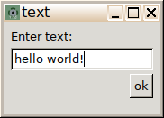
Over the drawing area, the cursor will show a capital 'A' in red to indicate how large the font would be. Click on where the text should be placed. A popup dialog will ask for the text data:

After clicking the 'ok' button or pressing enter, the text object is created on the current layer, using the current ("pen") text size and font. From pcb-rnd 2.4.0, route styles can specify a font too. When a style with a font specified is selected, it changes pen font to the style's font.
The text object can be moved around by the usual drag&drop operation.
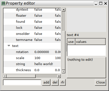
The following table provides a summary of the most common operations on text properties. Hotkey sequences are keys pressed in order, without the braces. The property editor can be invoked using right click on the text object, selecting the Edit properties menu from the popup.
| property | hotkey sequence | in the property editor | comments |
|---|---|---|---|
| text | {e t} | p/text/string | single line ASCII string |
| scale | {e g s}, {e g SHIFT-s} | p/text/scale | size ratio compared to the default 100 |
| rotation | n/a | p/text/rotation | CCW, in degrees; text is usually rotated within a buffer, when the whole buffer is rotated |
| thickness | n/a | p/text/thickness | when zero, an automatic value is determined from scale; when non-zero line and arc thickness within the text is set to this value |
| mirror | n/a | p/flags/onsolder | when the 'onsolder' flag is set, the text is drawn vertically mirrored; pcb-rnd sets this flag automatically when a text object is placed/moved to the bottom side of the board |
| font | n/a | font can be changed from the right click context menu, Change font... submenu. |

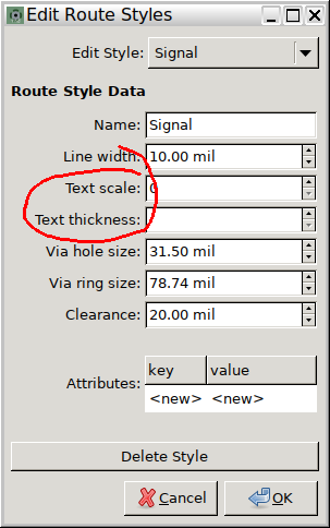
Each routing style has two fields, Text scale and Text thickness which are applied to any new text objects placed while the routing style is selected. These two fields affect the p/text/scale and p/text/thickness properties.

Subcircuit refdes: typically a silk text object that is part of a subcircuit, marked to be a floater and is a DYNTEXT with a template reproducing the "refdes" attribute of the parent subcircuit. When the string of such a text object is edited (with {e t}), pcb-rnd offers the choice to edit the DYNTEXT template or rather edit the refdes attribute of the subcircuit. The latter is the more common operation.
Polygon clearance: pcb-rnd does not calculate the clearance accurately, but it draws a rectangular cutout around the bounding box of the text.
There is no explicit property to write inverted text, but it is possible on non-copper layers using layer compositing.