Recent improvements to pcb-rnd include the ability to fine tune footprint parameters on the fly, even while working on a PCB layout, in an intuitive and simple to use parametric feature editing dialog window.
The library dialog is invoked by pressing the {w l} key sequence while editing a layout.
The pcb-rnd user has the ability to then browse the local filesystem libraries, specify and edit a parametric footprint, or retrieve a footprint from a web based repository if it has been specified in the preferences.
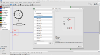
Here's a resistor being specified parametrically for a layout being edited:

Here's a BGA footprint being specified on the fly:

Here, a standard BNC footprint is being added from the local library residing in the local filesystem:

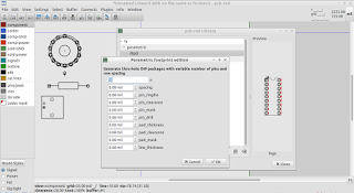
And here's a parametric DIP socket being specified on the fly in the parameter editing window:


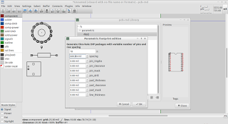
A fatter than usual DIP has been created and placed on the layout:

In addition to the options of standard, inbuilt footprint libraries, and parametric footprint creation, pcb-rnd has had the ability to retrieve symbols from web repositories for some time.
Once a compatible web based repository has been specified, pcb-rnd checks for updates and caches a list of the available footprints whenever it starts up.
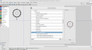
Here's a nixie tube footprint retrieved from gedasymbols.org. The nixie tube footprint was originally converted from a KiCad library, if memory serves correctly:

Importantly, any of the parameters generated interactively can also be embedded as footprint attributes in netlists exported by schematic editors, allowing parametric footprints to be specified from the schematic for automatic inclusion in the new layout.
A simple example for gschem, the gEDA project's schematic editor, would be the following attribute for a resistor:
footprint=acy(300)