| Name | Last modified | Size | Description | |
|---|---|---|---|---|
| Parent Directory | - | |||
| Abstract | 2017-12-25 04:51 | 132 | ||
| Author | 2017-12-24 04:53 | 26 | ||
| Body.html | 2017-12-24 04:54 | 3.3K | ||
| Cdate | 2018-03-16 19:48 | 11 | ||
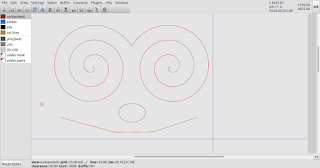
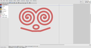
| Original-In-Inkscape.png | 2017-12-24 04:53 | 27K | ||
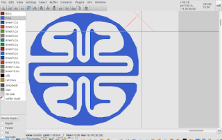
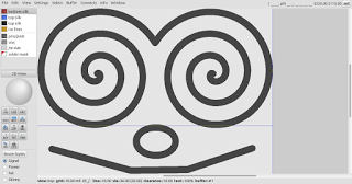
| Silk-Elements-Shifted-To-Copper-in-gEDA-PCB-RND.png | 2017-12-24 04:53 | 34K | ||
| Tags | 2017-12-25 04:51 | 44 | ||
| Title | 2017-12-24 04:53 | 88 | ||
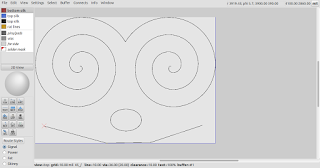
| exporting-from-inkscape-to-geda-pcb-rnd-layout.png | 2017-12-24 04:53 | 20K | ||
| gEDA-PCB-footprint.png | 2017-12-24 04:53 | 22K | ||
| inkscape-export-geda-pcb-rnd-layout-footprint-options.png | 2017-12-24 04:53 | 21K | ||
| inkscape-to-geda-pcb-rnd-export-with-line-thickness-option.png | 2017-12-24 04:53 | 22K | ||
| line-thickness-option-in-geda-pcb-rnd-export.png | 2017-12-24 04:53 | 34K | ||