pcb-rnd knowledge pool
New slot support in padstacks
| slot_ann by Tibor 'Igor2' Palinkas on 2018-09-10 | Tags: announcement, slot, padstack, plated, unplated, cutout, oblong, oval |
Abstract: Announcement of slot support. Example file with slotted padstacks and explanation of how using slots differ from the original pcb-rnd setup.
Boundary and mech layers are used to specify plated and unplated cuts/routes, including whether a layer is intended for board outline or slots. The idea here is that storing our objects on multiple layer groups, capturing a lot of details about their purpose, and then merging those layer groups on export (e.g. using the CAM plugin) is much simpler and straightforward than throwing everyting onto a single "outline layer" and then trying to tell them apart by heuristics.
The first use of this new layer type setup is slots. Below is a screenshot of the first slot example board:
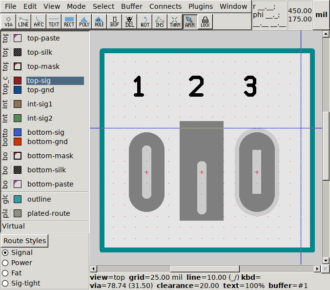
The first padstack is the classic, common case: oblong pad on all layers and a thru-hole slot instead of a hole. Typical for power jack connectors. The second example shows that there's no restriction on where the slot is placed within the padstack and the shape does not have to be the same as any other layer's shape. The third one is a rather special case to demonstrate the flexibility: it has different shape on the bottom copper to make more robust wave soldering and has a rectangular cutout for the slot. It is also marked as an unplated slot.
The padstack editor dialog is already updated, you can explore and tweak the padstacks: right click, edit geometry/prototype, second tab in the dialog.
Observations
1. a padstack being a slot is much less special than it first sounds, and this is how it connects with the layers: a slot is just a shape on a MECH layer type. This means the shape on the MECH layer, the shape of the slot, can be anything a padstack supports, including arbtitrary polygon. (And yes, it is possible to produce those: just look at any 80's VCR, with single sided board punched through for the slots)
2. The only special case is: you can have either a slot or a hole in a padstack, but not both. In theory the hole is not needed anymore, because a slot can emulate a hole, but because of 99.999% of the use cases, including vias, will need holes, I decided to keep the hole concept. It's sort of an optimization (just like the whole padstack is - the generic, constructive solution being heavy terminals).
3. bbvia aspect: the same code that is good for blind/buried via holes is good for slots too, so I decided to allow them. This means you can create blind or buried slots. I am not sure how many other EDA tools supports this (probably only a few) and whether fabs would do it (in theory it's just an extra routing/milling step), but as it just worked automatically, I won't remove it.
4. Plating: a hole or slot is either plated or not. Because of a known bug, connection find will always assume all copper shapes of a padstack is connected, even when a padstack is marked unplated (or the hole doesn't touch a shape). So at the moment this bit is mostly used for knowing in which file to export it.
5. I am slowly making things explicit. Like PCB "always" had an explicit silk layer (well, not in the 90s): we could draw on while elements also had side effects on. But in pcb paste and mask was side-effect-only, you couldn't draw on them. Then in pcb-rnd paste and mask layers became the same as silk, drawable. You even have control over which layer the side effects use (the AUTO layers). We still have some side effects not controlled that way, tho: drills. Now that we are getting explicit MECH layers, this will change. For slots it already works: if you turn off the visibility of outline (the unplated route in the test design) or plated-route, the slots being unplated or plated will disappear. Some time in the future drills will do the same.
6. slotting in padstack is the "light terminal" approach. It covers the most common, simple cases only. For more complicated cases you can always use heavy terminals or hand drawn explicit objects on layers. For example you can draw on the plated route layer and it will just create what the layer says, plated, routed cutouts.
7. There's a slight tweaking on the rendering engine to make sure slots, outlines and generally any mech layer ends up on top in the rendering.
8. Reminder: we have layer groups that refer to physical layers and hold the physical properties, and we have layers which are just canvases contributing to a layer group's rendering. Anything important about how a layer group behaves, what it describes and how it will be fab'd is stored in the layer group. We go by fields, not name: you can name both the group and the layer anything you want.
9. Multiple outlines: the code had this limitation until yesterday: you could have only one outline layer. As far as I can tell, I've removed this from all parts of the code. You can have multiple layers packed into a single unplated routed layer group (or any other group). We won't allow compositing tho, because we need to determine non-polygon shapes and fabs will want centerline route data too, which compositing would make very hard. So routed mech layers are always positive, just like copper layers. The main uses of multiple layers is having multiple colors and allowing subcircuit/buffer layer binding trickery. For example if your subc has two slots for different purposes and they are specified on different layers within the subc, you can decide to omit them by purpose, using the layer binding dialog, redirecting some of those layers to invalid.