pcb-rnd knowledge pool
How to export for macrofab
| macrofab by Edward 'celem' Comer on 2018-01-28 | Tags: howto, fab, p&p, pick, place, export, gerber, xy, xyrs |
Abstract: How to export files from pcb-rnd for macrofab pick and place service.
Creating Macrofab Compatible Files with pcb-rnd
Macrofab requires Protel-like suffixes . Macrofab has a help page that explains their requirements at THIS-LINK . For example, the Top Copper layer's suffix is GTL, i.e., filename. gtl
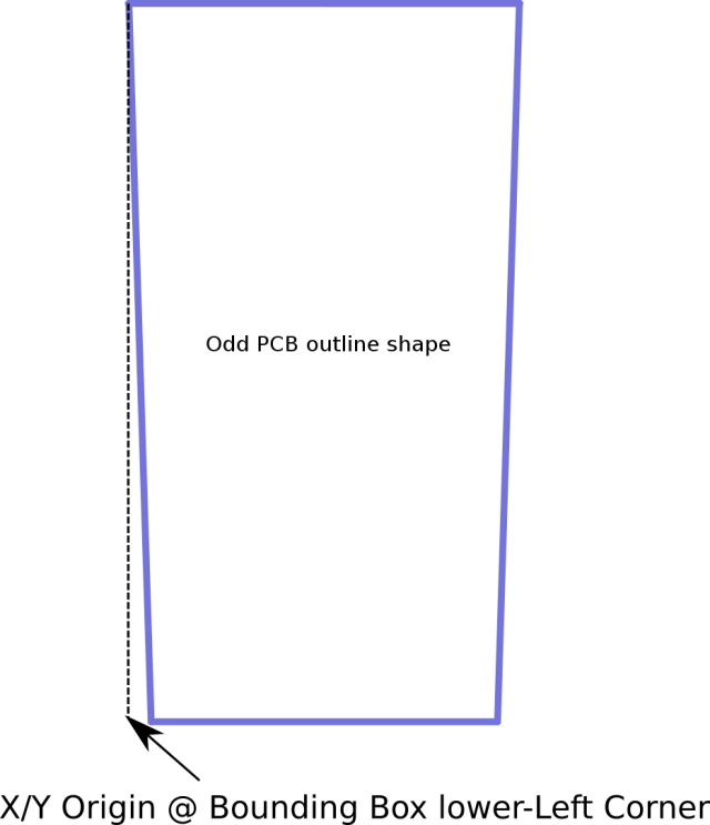
- By default pcb-rnd uses the implicit Pick and Place(P&P) origin of 0;0 at the lower left corner. This would work automatically with square/rectangle boards.
- pcb-rnd also offers an explicit, user defined pnp origin; this shall be used for odd shaped boards. This origin used for XYRS files with a special mark on any layer of the board - a "pnp-origin" Mark.
First create macrofab compatible files
-
You will be more successful if your pcb-rnd
layout includes certain fields for your board. Consequentially, make sure
that your layout is production ready before starting this proces:
- Your part's footprint and value attributes (Edit -> edit_attributes_of -> subcircuit) should be meaningful. This is because macrofab will need real manufacturer part numbers and values (ohms, etc).
- Macrofab's Bill of Materials screen can search parts that are available from component vendors but if your part number is a real manufacturer's part number and value then the process will go much more smoothly.
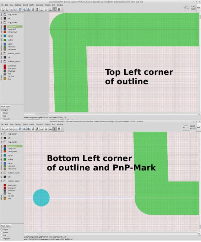
- The pnp-origin dot is created by drawing a short, thin line and then drag&drop move the endpoint of the unselected mark line back to its origin endpoint - this will result in a zero length line, which looks like a small filled circle.
- Next select the dot, drag&drop move it to be centered on the lower left corner of the outline box relative to the board outline's line centerlines ( bounding box ).
- With the mark still selected, press ctrl+e and click on the "add attribute" button in the property editor.
- Type in "pnp-origin" in the "Attribute key" and "yes" in the "Attribute value" field; click ok and then close the property editor. A short video of pnp-origin creation is available at THIS-LINK .
- Finally, export the Gerber and xyfile:
- When exporting the gerbers (File -> Export_Layout -> gerber), select checkbox "all-layers" and select name-style "universal".
- When exporting the XY file (File -> Export_Layout -> XY), select "Macrofab" format. Rename the XY file's suffix to XYRS.
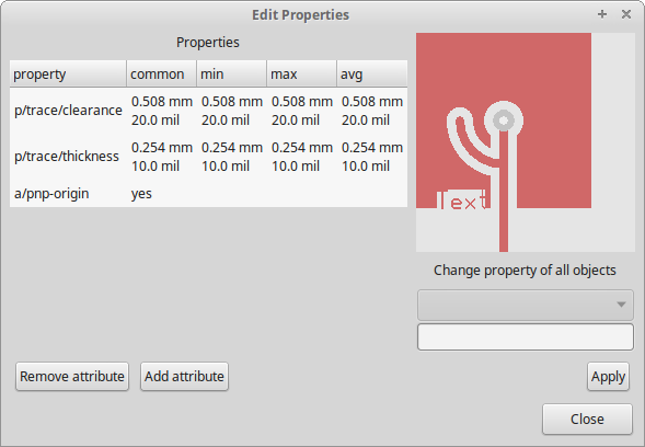
Note 1: The pnp-origin mark is not explicitly visible in the XY file nor is it explicitly passed to macrofab. Instead, all part coordinates are calculated considering the mark's center as 0;0.
Note 2: However, the mark is not hidden or suppressed by pcb-rnd from any of the output. It must be a line, but it can be on any of the layers. Thus the mark potentially could show up on the board. There are options to make the mark disappear:
- Make the mark diameter smaller that the router mill bit diameter and place the mark on a copper layer; the board fab will have the copper dot, but it will be milled away.
- This should also work if the mark is on a silk layer or even on the solder mask layer where this object would be a small cutout over void
- Make a new (copper) layer or unused layer, such as an inside layer, place the mark there and don't send that layer's Gerber export to macrofab.
Controling the last two columns
The last two columns of a macrofab xy are "Populate" and "MPN".
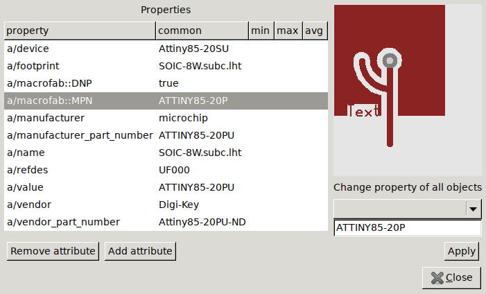
The "Populate" column is 1 by default, directing macrofab to populate the part. It can be changed to 0 if the given subcircuit has an attribute "macrofab::DNP=true" set.
The "MPN" column is "n/a" by default. It can be changed to an arbitrary part number using the "macrofab::MPN=partnumber" attribute.
The easiest way to set these attributes is selecting the subcircuit, or multiple subcircuits that are going to have the same value, and invoke the property editor (ctrl+e). Adding new attributes is possible using the 'Add attribute' button.
Next Upload Files to macrofab
Macrofab has help pages that explain their process for uploading and verifying board files to their system for several EDA software products but not specifically for pcb-rnd. If your board is created as described above you should have no problems.