pcb-rnd knowledge pool
Using and editing lines on layouts in pcb-rnd
| line_edit by Erich Heinzle on 2018-01-17 | Tags: howto, line, edit, clearance, route, styles, all, direction, menufile, menuv1 |
Abstract: Show how lines can be drawn, modified, and how various settings affect their use.
How to create and modify lines in pcb-rnd
Unlike some EDA packages, pcb-rnd treats lines as simple geometric features with no associated electrical "Net" that imposes restrictions on line characteristics.
Lines are the simplest way to implement tracks on PCB layouts, as well as board outline geometry, artwork on the silk screen layer, or apertures in the solder mask layer.
The line tool behaves much like a line tool in other two dimensional drawing software.
The line tool can be selected from the menu:
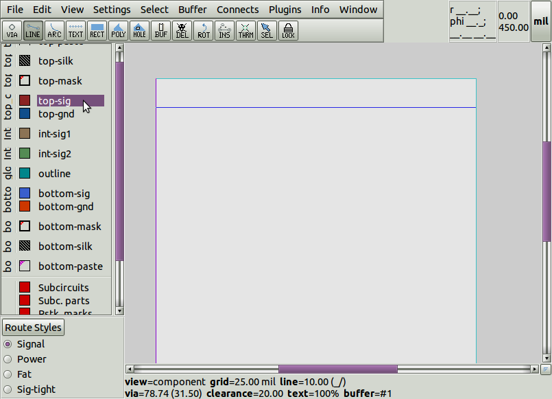
The intended layer for the tracks needs to be selected too, which will typically be a copper, silk or outline layer
The line can be started with a click of the mouse or trackpad at the desired location:
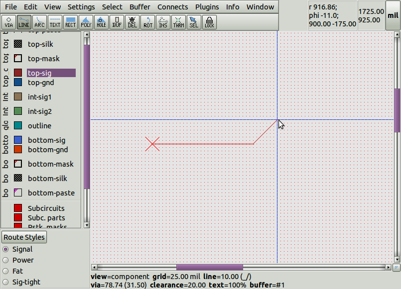
the line will then extend to where the mouse pointer goes, and pcb-rnd will add 45 degree bends to the line to meet the cursor. The direction of the bend can be flipped by holding the SHIFT key (can be "permanently" toggled using the '/' key):
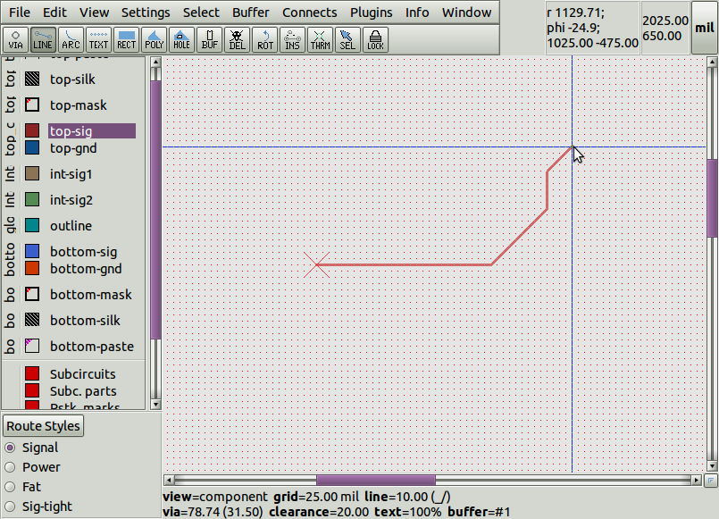
Clicking once more lays down the positioned trace
At this stage, the last point remains an origin for further routing if required, that continues from that point
The continued trackwork can then be laid down with another click:
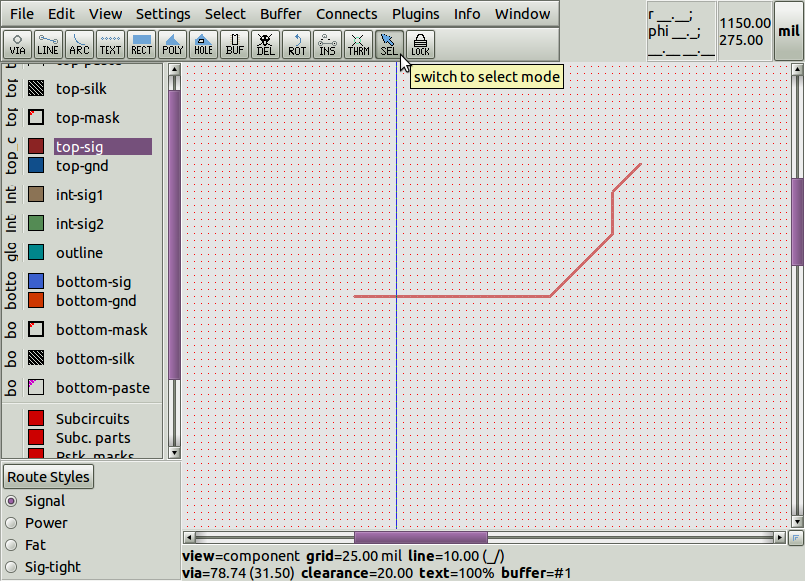
Once the tracks have been laid, the line tool can be exited by using the ESCAPE key or clicking on the select tool:
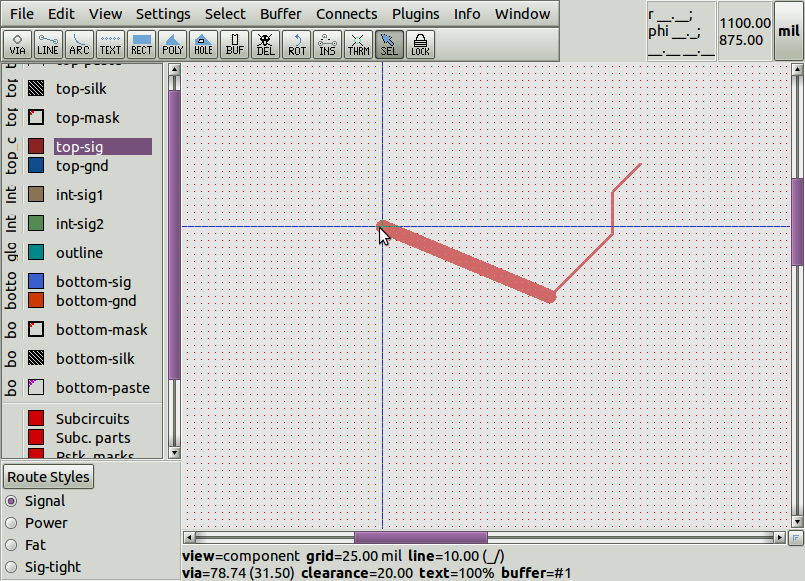
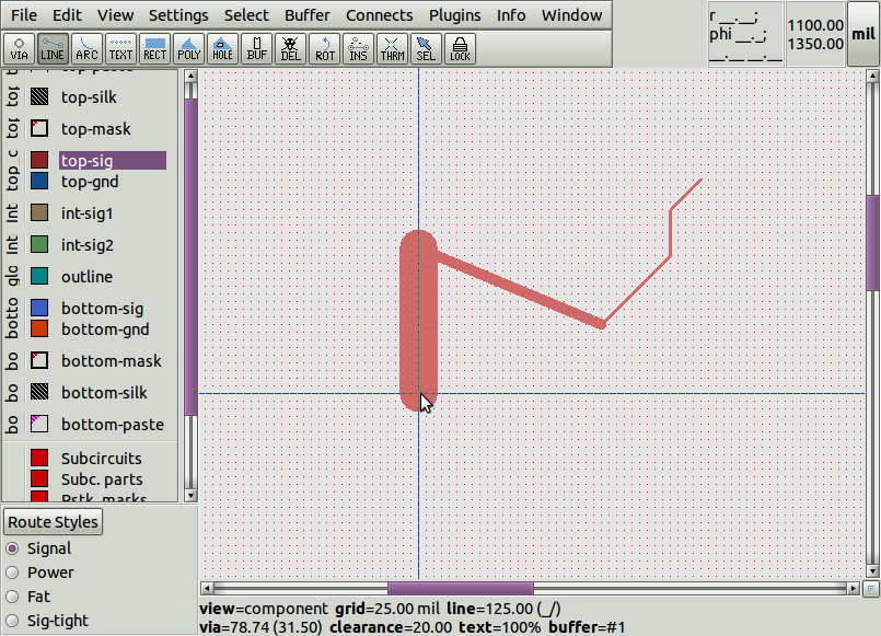
By holding the mouse over a track and using the e, g, s key sequence (written as {e g s} for short), the track can be fattened:
The cursor will snap to the end point of lines automatically, allowing the user to continue laying further tracks easily, or modify the existing track:
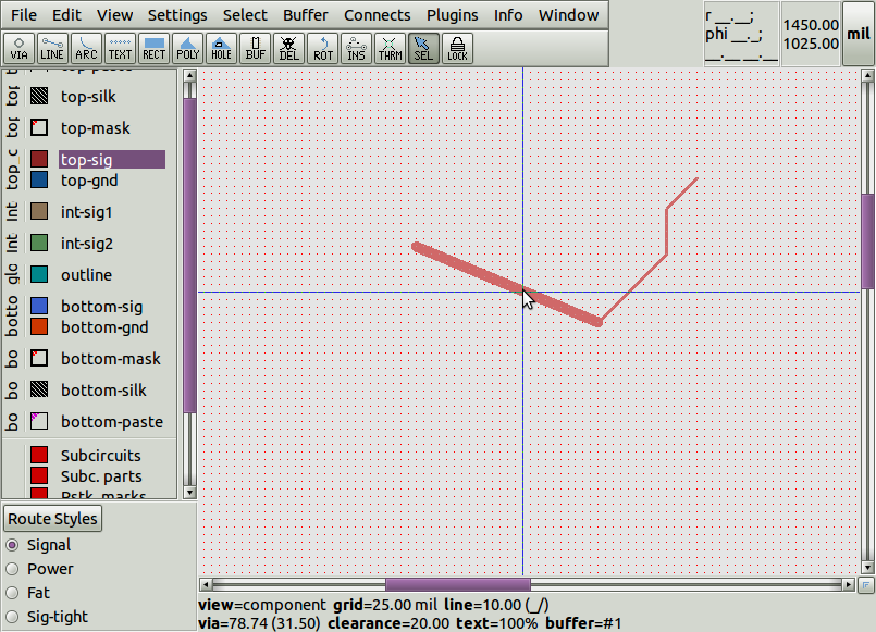
Clicking and dragging on the end of the line with the select tool allows it to be moved:
with the cursor over a line, {e g SHIFT-s} will make the line thinner; the opposite effect of the {e g s} key on a line
In addition to using {e g s} key to modify the thickness of individual line segments, the "Route Styles" settings can be used to modify the thickness of lines currently being drawn with the line tool.
Routing styles
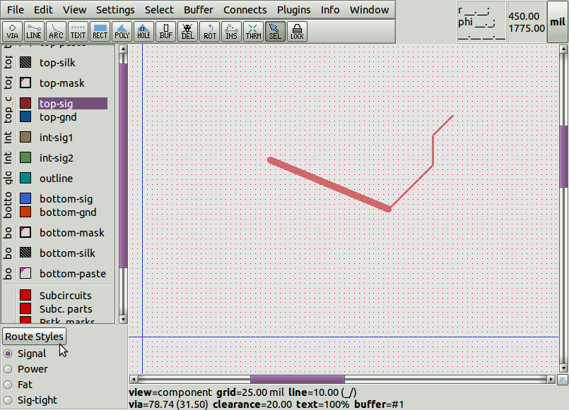
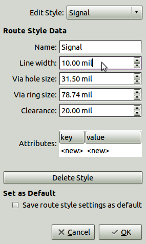
pcb-rnd has four route style settings by default (more can be added), any one of which can be selected for drawing and/or modified if required:
In this case, we make the normally "thin signal" style thicker to demonstrate
and we see the effect on a line drawn with the signal route style:
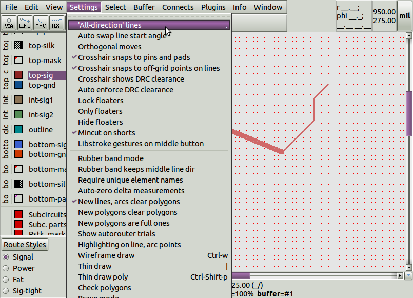
all-direction lines
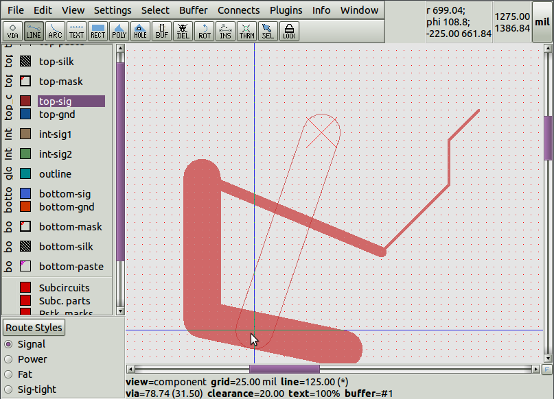
The all-directions line setting in the menu allows lines to be drawn at angles which are not just multiples of 45 degrees (can be toogled using the {.} key):
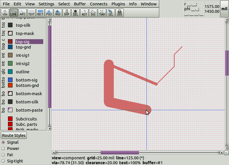
This allows traces with an arbitrary line angle to be drawn:
snapping
The line tool will also snap to the midline of existing lines that are grid aligned, simplifying completion of connections:
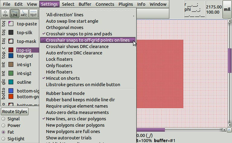
but for this to work on lines at arbitrary angles, the "snap to off grid point on existing lines" menu option needs to be selected:
clearance
The clearance of a line can be easily adjusted by using the {e g c} and {e g SHIFT-c} keys when the cursor is over the line.
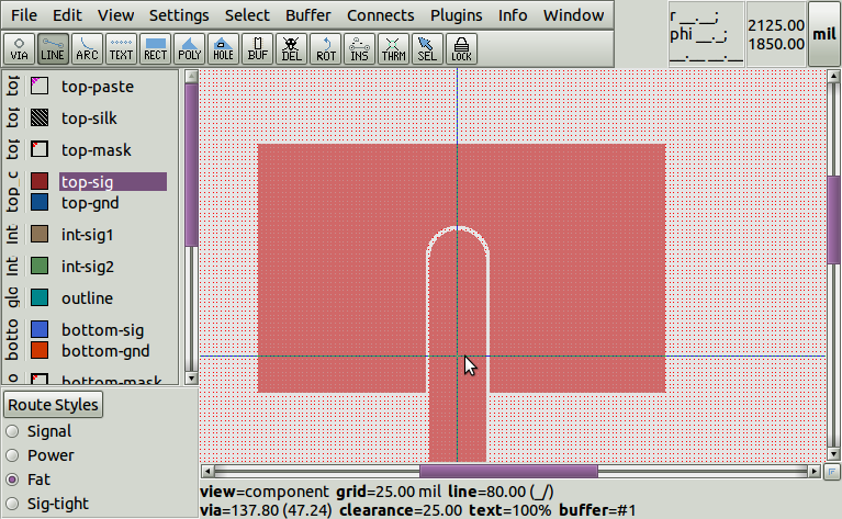
Here is the original clearance visible around a line laid across a polygon:
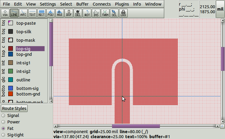
The {e g c} key is used to increase clearance:
and {e g SHIFT-c} is used to reduce clearance:
Further {e g SHIFT-c} use ultimately extinguishes the clearance completely, electrically connecting the track to the polygon:

