pcb-rnd knowledge pool
Converting inkscape paths to pcb-rnd and gEDA PCB layouts, lines and footprint elements
| inkscape by Erich S. Heinzle (VK5HSE) on 2017-03-20 | Tags: howto, import, svg, inkscape, art, artistic |
Abstract: Introduction to an Inkscape export plugin that can (partially) export svg to .pcb, creating a bridge between inkscape and pcb-rnd.
Inkscape is a powerful FOSS vector graphics tool that allows editing of complex paths which can then be exported to various formats.
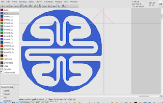
Being able to export paths to PCB layout software is useful for a number of reasons, such as enabling custom or artisanal board outlines and tracks to be implemented, such as the following flying spaghetti monster (FSM) designed with pcb-rnd and FidoCadJ :
or allowing intelligent design of exotic footprints like the following touch pad example:
After looking at an Inkscape HPGL export module written by Aaron Spike, a pair of python modules were written, based on the Inkscape's HPGL exporter.
These extension scripts are available from:
https://github.com/erichVK5/inkscape2pcb
and the *.py and *.inx scripts need to be copied (you'll probably need sudo / superuser privileges) into your local inkscape extensions folder, i.e.
/usr/share/inkscape/extensions
After starting Inkscape up again, and creating a design...
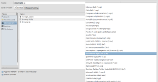
...you should have the options to export to both gEDA PCB footprint (.fp) format, and to pcb-rnd layout (.lht) format available in the "Save As:" menu:
The paths in the layout are automatically flattened and converted to line segments in the exporter:
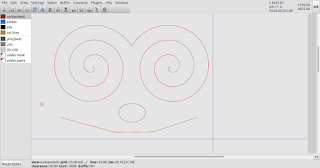
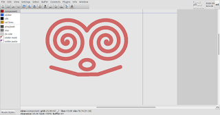
Here's the exported layout being viewed in pcb-rnd, the fork of gEDA PCB:
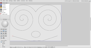
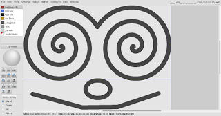
And here's the layout exported as a footprint, being viewed in gEDA PCB.
Naturally, KiCad users can use the same scripts to export footprint designs, since KiCad can import gEDA PCB footprint (.fp) natively.
There may be scope to improve the code by implementing export of solid polygons, but more needs to be learned about Inkscape's internal data structures first.
Support for specifying line thickness has also been added to the export dialog, and can range from 8mil (default) to 250mil (mil being thousands of an inch, a.k.a. thou, a.k.a. 254 microns, a.k.a. 0.254mm). This is a fairly sane range of values, but the thickness can always be changed in gEDA PCB or pcb-rnd if necessary.
The scripts have been tested with "px" as the default unit of measurement in Inkscape. One "px" maps to one mil in gEDA PCB and pcb-rnd; users will need to confirm that exported dimensions are maintained when exporting; if not, the dpi setting could be experimented with for scaling during export.
In closing, it should be mentioned that accurate geometry in Inkscape is most easily achieved by individually clicking on nodes, and then manually entering their required coordinates.

