pcb-rnd knowledge pool
How to add a ground pour to a layout
| ground_pour by Erich Heinzle on 2018-01-17 | Tags: howto, pour, copper, ground, plane, pullback, clearance, routing, menufile |
Abstract: Show how a ground plane (a.k.a. copper pour) can be added to a layout.
How to add a simple rectangular ground plane (a.k.a. copper pour) to a layout in pcb-rnd.
A ground plane, as the name implies, is an area of copper on the PCB that provides a common ground for connection to all grounded component leads. Ground planes can simplify routing, and can also add stability to RF circuits.
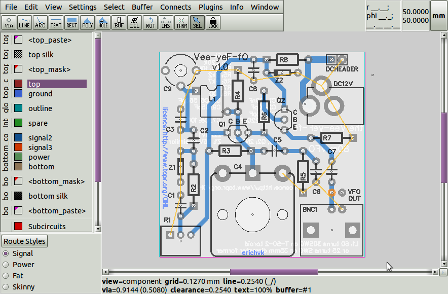
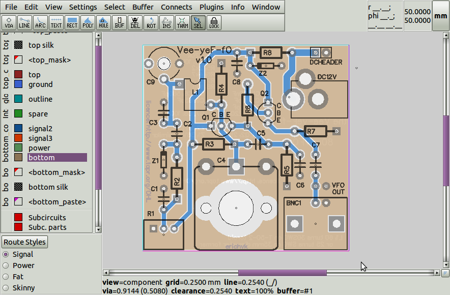
The required routing on the board can be continued with tracks up until the point the ground nodes remain the only items that need to be connected. The following picture shows the rats nest lines at this penultimate stage:
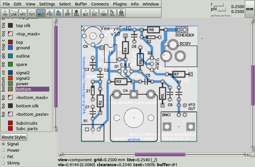
Having done this, we now click on the rectangle tool.

We next select the active layer where we intend to place the ground pour.

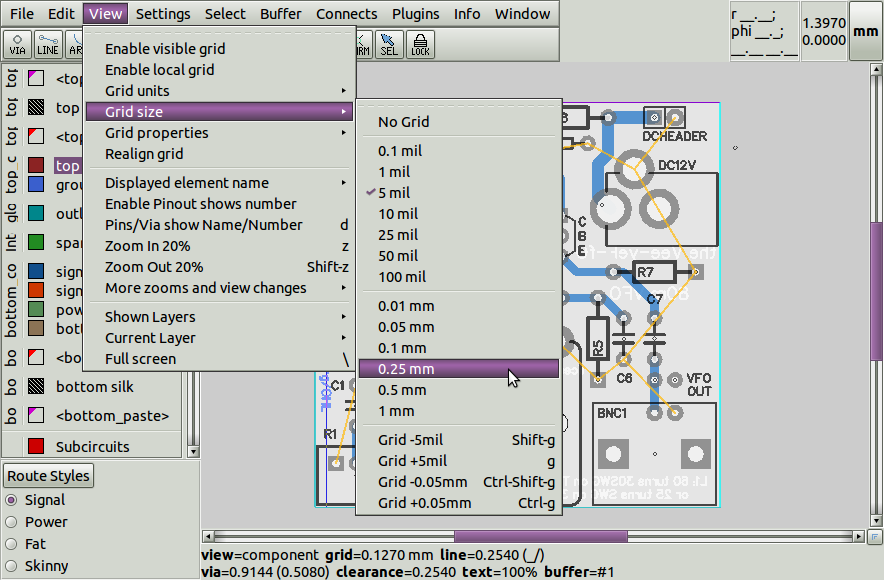
Most PCB manufacturers will require a "pullback" of 200um (.2mm) from the edge of the board to prevent tearing of copper features when boards edges are milled or cut. The simplest way to achieve the required pullback is to select a grid size to suit. In this case, a grid size of 0.25mm will allow the 0.2mm minimum pullback required by the PCB manufacturer to be drawn quickly and easily, and we select it from the menu.
We can now start with the first corner of the rectangular copper polygon by clicking at (0.25mm,0.25mm):
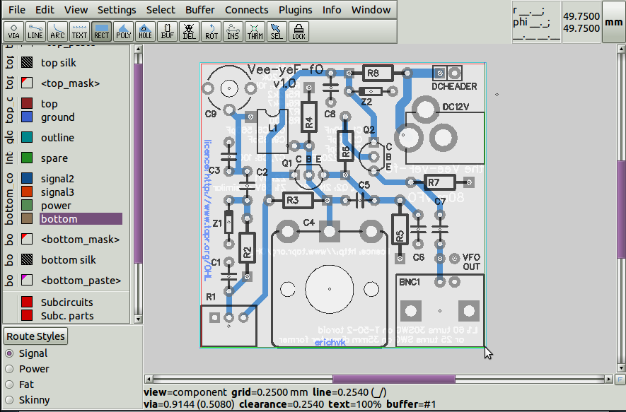
We now click to create the opposite vertex to create the pour with the required pullback:
At this stage, all that remains is to run a design rules check (DRC) to ensure that board routing is complete.
An obvious question is "Can I do the pour first, and then route the tracks?". The answer is yes, both orders can be done. Some users find it easier to place the pour near the end of routing, as attempts to lay track on the same layer as the polygon may lead to connections where clearances between the pour and the laid tracks are in fact intended. Other users prefer to start with the polygon and lay down tracks on it; this allows seeing how clearances will cut the polygon into islands while routing the board.
More complicated pours for non rectangular boards can be achieved using the polygon tool instead of the rectangle tool (but both tools result in a polygon object).
Note: we assumed all objects on the board are clearing polygons; this depends on a flag (usually CLEARLINE) and the object's clearance value being greater than zero. With default settings both are true, but both can be changed - if an object "disappears" under a polygon, check the object flags and clearance value.
A 3rd way an object can interact with a polygon is called thermal .
Note: unlike in some other EDA tools, in pcb-rnd polygons are not bound to networks in any way. Drawing a polygon will not automatically assume the polygon is (or should be) connected to ground or power. Network connection is only an imaginary concept mapped dynamically: the same polygon object can be part of the ground network now, then after removing a few other objects to disconnect it from the ground and draw some other objects to connect it to a signal network, can become part of a signal network.