pcb-rnd knowledge pool
Exotic and complex footprint creation using FidoCadJ
| fidocadj by Erich S. Heinzle (VK5HSE) on 2017-03-09 | Tags: howto, file format, format, fidcad, convert, art, artistic, footprint, curve, curves, menufile |
Abstract: Sometimes there are complex or exotic footprints that need to be made which are most easily achieved with bezier curve, cubic spline and ellipsoidal features in addition to the usual rectilinear elements. Fidocadj is a CAD program good in those. This howto demonstrates the bridge between pcb-rnd and fidocadj.
Sometimes there are complex or exotic footprints that need to be made which are most easily achieved with bezier curve, cubic spline and ellipsoidal features in addition to the usual rectilinear elements.
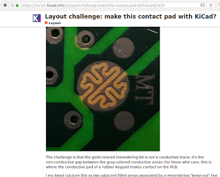
A good example of one such footprint came up on the Kicad forums; a contact pad for use with rubber dome pushbutton switches which have a conductive underside which shorts out the gap in the exposed pad:
The fairly symmetrical design and filleted features are a natural fit for the cubic bezier, ellipsoid and cubic spline support in FidoCadJ, the no nonsense 2D cross platform CAD package which now has an export module for exporting these design features as line elements in a pcb-rnd (or gEDA) layout.
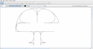
The design was fairly quickly prototyped in FidoCadJ at a scale that suited the features. It should be noted that on export, FidoCadJ allows a magnification factor to be provided to allow the design to be magnified or shrunken, so the 5mil grid in FidoCadJ never becomes a limitation.
The design was executed on the "circuit" layer in FidoCadJ, since this is the default layer, and when exported to pcb-rnd format by the export module, is exported to the rear silk layer with 10mil lines by default.
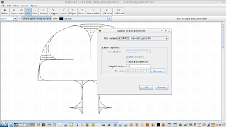
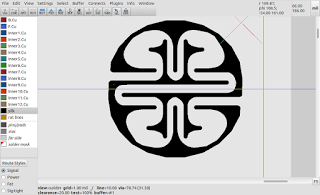
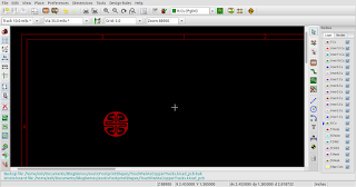
After creating the outline and the interlocking features with cubic splines and lines, the internal, open portions were hatched with additional lines to act as fill. Following this, the layout was exported to a gEDA PCB (.pcb) layout using a magnification ratio of 0.18, which generated a footprint of the desired dimensions (~ 6mm round):
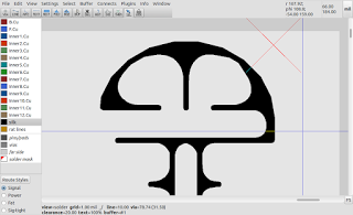
The exported layout was then loaded in pcb-rnd. The same exported file would load with gEDA PCB.
The layout can be flipped in pcb-rnd / PCB with the tab key, if the underside is to be viewed, as above.
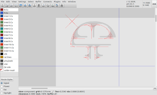
For an essentially round design such as this, a more uniformly contoured outer margin can be achieved by using an encircling ellipsoid, and deleting un-necessary line segments. This was ultimately done in this case, to create a more uniformly rounded appearance than cubic beziers were able to achieve.
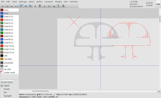
Looking at the line elements from the front, the elements were selected with Alt-A, and then Ctrl-C was used to copy them into the buffer:
This design has point symmetry, enabling the copied elements to be mirrored twice, or rotated, to complete the other half of the footprint. The buffer contents were mirrored Left-Right:
and the buffer was then mirrored Up-Down:
The transformed buffer elements are then placed where they belong, completing the basic design. Some of the "fingers" were lengthened a little to fine tune the spacing, and any residual gaps in the hatched areas were filled with additional lines:
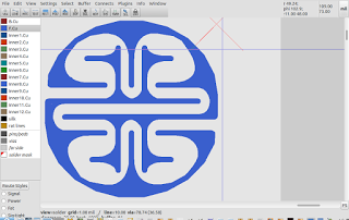
At this stage, the elements can be moved from the bottom silk layer to the front copper layer. First of all, the top copper layer needs to be selected in the layer list in the left dialogue of the pcb-rnd screen. Once the intended layer is selected, Alt-A is used to select all of the elements, and then "Shift-M" is used to move the elements to the top copper layer:
At this point, a KiCad pcbnew user can simply use the "Save As" dialogue to save the layout in either KiCad legacy or KiCad s-expression format, at which point it can be loaded into pcbnew for further manipulation:
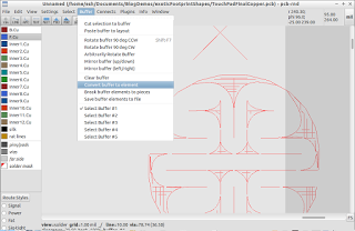
users keen to create a pcb-rnd compatible footprint can proceed to do so by again using "Alt-A" to select all of the elements, followed by "Ctrl-X" to cut the elements to the buffer. Ensure the cursor is over an appropriate centroid or origin for the planned footprint - in this case the centre of the element was chosen for the mouse pointer location when "Ctrl-X" was used:
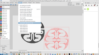
Using the "Buffer" menu, the buffer contents can be converted to a footprint with "Convert Buffer To Element" command:
Which results in the new element (footprint):
At this point the element can be saved to a footprint file:
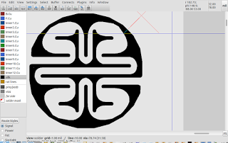
Here's the final result, a footprint being viewed in pcb-rnd:
The remaining work required for use with a netlist and design rules checking is suitable numbering of the overlapping pads, to end up with two distinct electrical groups of pads, numbered either pad "1", or pad "2".
In a complex footprint design like this (ultimately with 401 distinct pads!), this is most easily achieved by loading the footprint into a text editor and doing some search and replace on the consecutively numbered pads.
Alternative approaches to creating a footprint like this would include using pstoedit, or tracing outlines in a utility like inkscape, and then exporting in a format compatible with one's preferred PCB layout editor or an intermediate conversion utility.
The method described is efficient, and appears to be the quickest and least painful method for complex curve creation in footprints at present.
It is worth noting that FidoCadJ now has support for loading a background image, which, with suitable scaling of the image prior to use, can provide a background template for duplication with cubic bezier, cubic spline, line and ellipsoidal elements.
