pcb-rnd knowledge pool
Back annotation to gschem
| backann by Tibor 'Igor2' Palinkas on 2015-08-30 | Tags: howto, video, schematics, netlist, back annotation, back, annotation, gschem |
Abstract: Back annotation of pin swaps and footprint changes using pcb-rnd and a recent GIT version of gEDA/gschem.
| Update (2023) : gschem is still in hiberation with zero chance of cooperation. Meanwhile Ringdove offers a new schematics editor, sch-rnd . With the support from nlnet the back annotation system got a major upgrade (both in pcb-rnd and sch-rnd) and a section in the user manual . This pool node is still valid, but is outdated, describing only a subset of the features available. |
Update (2020) : after all, there was a gschem release and it should contain the back annotation.
( Update (2019) : gEDA is in hibernation, and gschem is already totally dead. There is no much chance for a new gschem release. While the workflow demonstrated below does work, with such a future of gEDA and gschem it is probably better to avoid investing time in this flow. There are plans to make back annotation available with other schematics editors. This article is kept to demonstrate how it should work.)
After a succesful forward annotation and partial routing, the user finds that two rats are crossing. The solution is swapping two pins on the netlist in pcb-rnd. The user also wants to replace one of the resistors with a smaller one - this is done by a few clicks too. The netlist patch is then saved and imported in gschem.
Gschem finds the outstanding differences, and assists the user to fix them on the schematics.
(original video on archive.org)
History of the feature
Back annotation was a long standing missing functionality. There has been different suggestions, including:
- back annotation is not needed at all, the user can do it manually
- pcb should generate a new netlist, the user should run diff on the netlists and manually edit the schematics
- gschem should be able to load netlists emitted by PCB; or gnetlist could reverse-process such a netlist
The current implementation allows pcb-rnd users to make deliberate pin swapping and footprint replacement. The changes can be saved in a "netlist patch" format. Recent GIT version of gschem can load these and present them as search results pointing to parts of the schematics that need to be changed.
The underlying mechanism is versatile and potentially allows more changes to be back annotated. These are not yet accessible due to the lack of pcb-rnd actions and GUI.
Design decisions
This devlog entry functions as a design decision document. Another entry is a summary on how the feature ended up in a private feature-fork of gschem.
save/load and compatibility with gEDA/pcb
As expected, gEDA/pcb didn't track the changes and did not take the code for the new feature. Thus in some situations it results in .pcb files that need minor manual edit before gEDA/pcb can load them.
Deliberate changes are tracked so that a new forward annotation from the old schematics won't break them. To do this, pcb-rnd saves a NetListPatch() section in the file. Mainline PCB can not handle this section. Compatibility, by use case:
- 1. No back annotation is made in pcb-rnd: the file stays compatible
- 2. Back annotation is made in pcb-rnd, then the changes are done on the schematics and a forward annotation is also done: the netlist patch in pcb-rnd becomes empty so the pcb file is again compatible with mainline pcb; this is called resolution of netlist patches
- 3. There are unresolved netlist patches saved in pcb-rnd and the user attempts to load the pcb file in mainline pcb: syntax error (but no data loss); solution: resolve the netlist patch as described in point 2.
- 4. Cheat for situation 3.: manually remove the NetListPatch() section from the save file. This way the back annotation info is lost, but mainline pcb can load the file again. This action is sort of "revert back annotation".
- 5. Any file saved by mainline PCB can be opened by pcb-rnd, back annotation does not affect that.
plans
Back annotation for further changes, e.g. value change, naming/renaming nets, etc.
technical details
netlists, annotations
Pcb-rnd (and mainline pcb) maintains a netlist as part of the design. Pcb doesn't modify the netlist. The netlist is imported from an external source, typically from gschem. This process is called forward annotation.
Sometimes there are a set of connections which contain pin pairs that could be swapped. For example the data lines of an external parallel SRAM interface to an MCU: it doesn't matter if data bit 1 at the MCU is wired to data bit 1 or 5 of the SRAM, as there is an 1:1 mapping and no one else is using the same bus wires. In this case connections should be swapped during pcb routing and annotated back to gschem so that the schematics can be updated. Both paths are illustrated below.
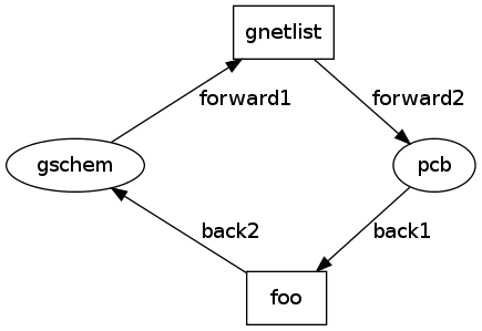
Forward annotation passes on complete netlists along arrows forward1 and forward2. Back annotation would pass back netlists, changes or modification requests on the back1, back2 path. Gnetlist takes sch files to extract and build a netlist in whatever format the receiver needs. There should be a glue layer, called foo on the drawing, that does the reverse: receives whatever format the sender has and generates something that gschem will understand.
Support in pcb-rnd: core
Pcb-rnd gets a complete netlist. If the user could change the netlist directly, there should be some sort of diff tool in foo that can explain the changes to gschem, or a diff tool in gschem. What is worse, forward annotation happens much more often than back annotation and pcb-rnd would need to be able to merge a new netlist with local changes. The simple "gsch2pcb overwrites the netlist in pcb from whatever gnetlist produced" approach would not work.
An alternative is to keep the netlist as-is, and maintain a separate list of changes. The form proposed hereby is a table of "operation,pinID,net" or "operation,args...". Netlist operation is one of "del_conn", "add_conn" and "net_info". The table is called the netlist patch .
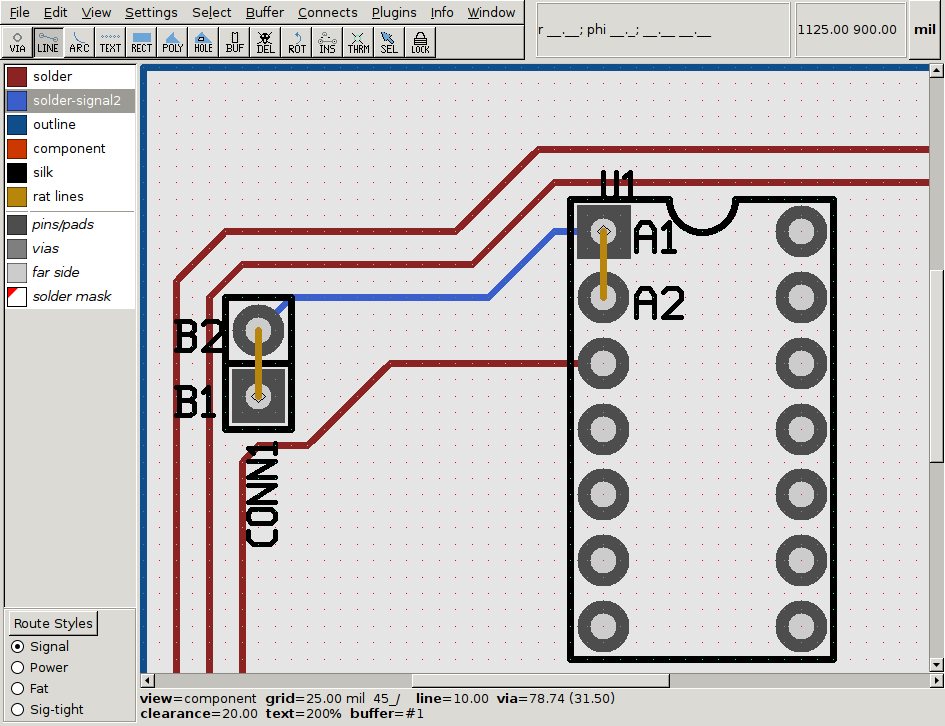
For example assume two components with pins A1, A2 and B1, B2, with connections n1=A1-B1 and n2=A2-B2. While routing the designer decides changing them to n1=A1-B2 and n2=A2-B1 would be easier and is acceptable by the design. The table of changes would contain this:
| op | pinID | net |
|---|---|---|
| del_conn | B1 | n1 |
| del_conn | B2 | n2 |
| add_conn | B2 | n1 |
| add_conn | B1 | n2 |
Pcb-rnd would store this table in memory. When some code calls the netlist code to find out the members of a net, or which net a given pin is connected to, after running the original netlist code, the result would be adjusted by the table.
The table would be normalized after operations. For example:
| op | pinID | net |
|---|---|---|
| del_conn | B1 | n1 |
| add_conn | B1 | n2 |
| add_conn | B1 | n3 |
| del_conn | B1 | n2 |
| op | pinID | net |
|---|---|---|
| del_conn | B1 | n1 |
| add_conn | B1 | n3 |
Pcb-rnd would save the normalized table in the pcb file in a new section. Upon a netlist change in pcb (import/load netlist or load the pcb), pcb-rnd would check each row of the table: it is easy to decide whether that row has been implemented in the netlist or not. Obsolete rows of the table would be deleted.
A corner case is when B1 is removed from n1 and then added to n2 by the table, while a new forward annotation removes B1 from n1 and adds it to n3. In this case the first row of the table is deleted, as B1 is already removed from n1, but pcb-rnd has no chance to decide if netlist adding B1 to n3 should affect the table adding B1 to n2, so that rule is kept.
net_info is used to describe the original members of a net, in the state they were before any change on the netlist occurred.
Support in pcb-rnd: GUI
A trivial idea is to extend the netlist window so that pins can be moved in between nets or deleted or assigned to nets. Changes should be marked. This is not the preferred way of editing the netlist, tho: not much more convenient than making changes in gschem and doing forward annotation.
There should be a separate dialog box or a separate region of the netlist box showing the netlist patch with edit capabilities.
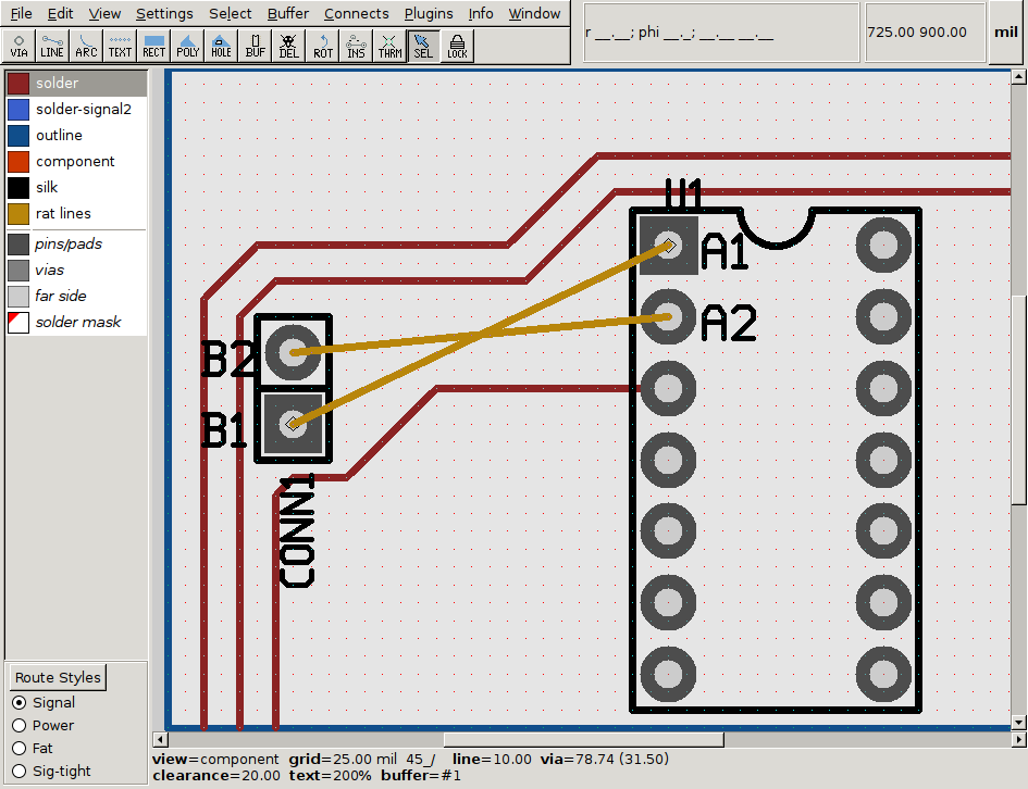
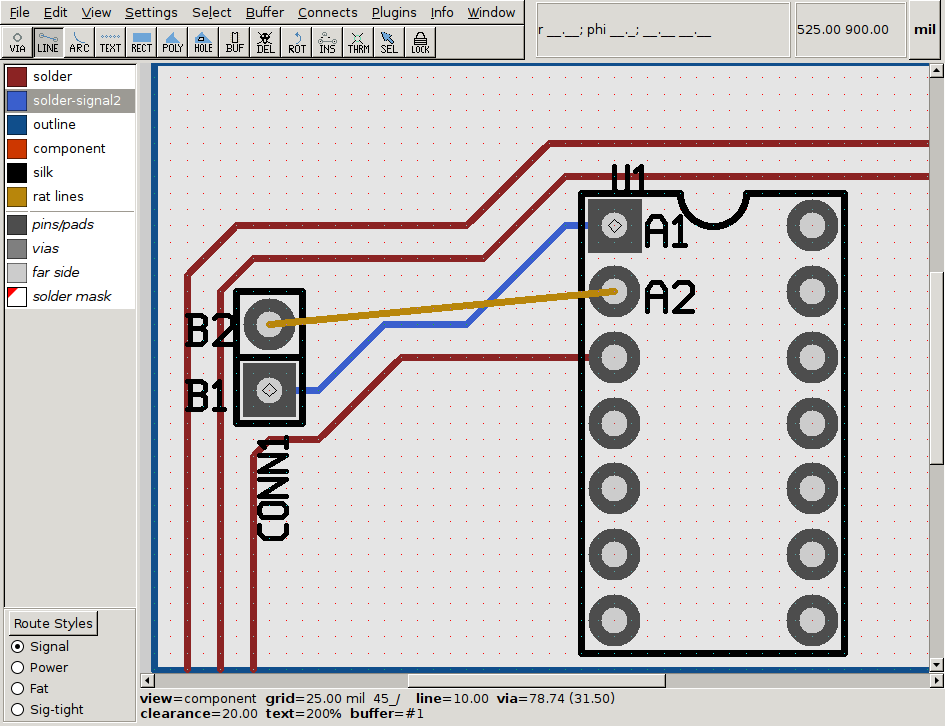
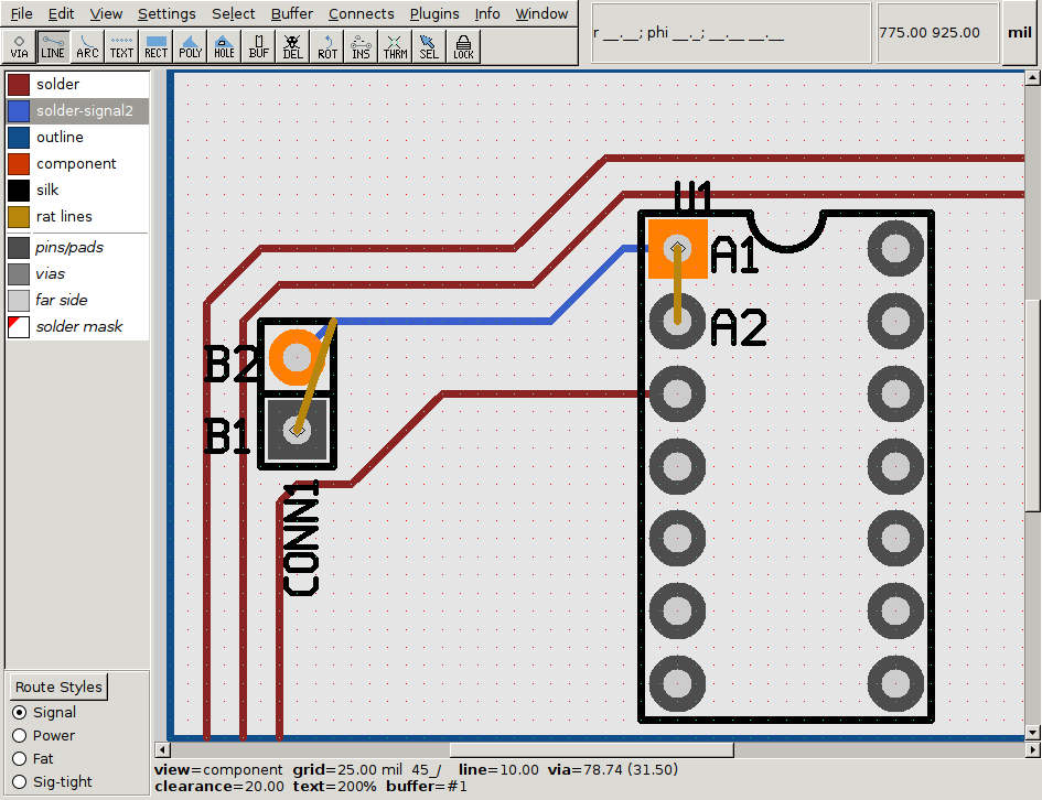
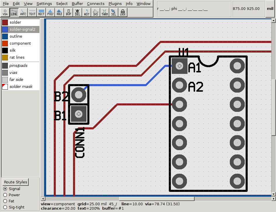
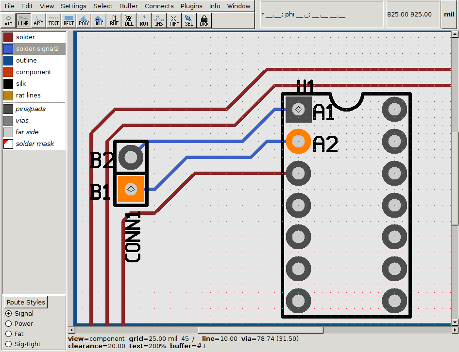
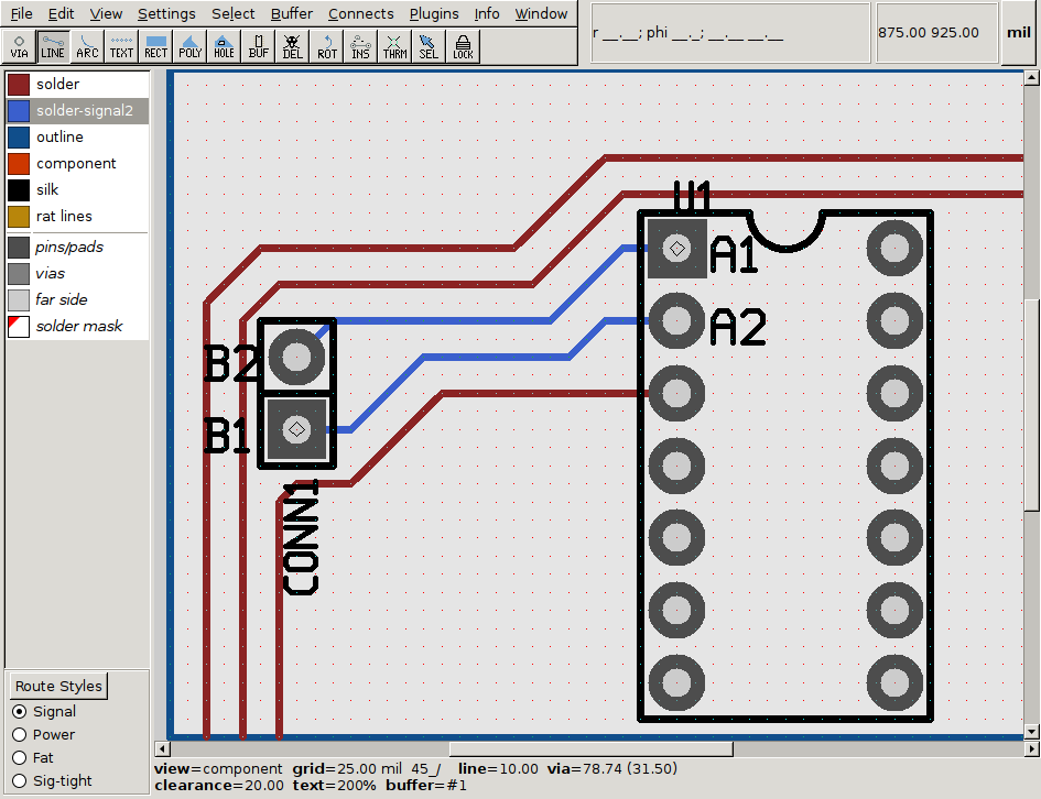
Finally, the most important feature would be new actions resolving shorts. Using the above example (n1=A1-B1 and n2=A2-B2 changed to n1=A1-B2 and n2=A2-B1), I believe the user would:
| action | screenshot | patch list after the actions |
|---|---|---|
|
| (empty) |
|
| (empty) |
|
| (empty) |
|
|
net_info n1 A1 B1 net_info n2 A2 B2 del_conn B1 n1 add_conn B1 n2 |
|
|
net_info n1 A1 B1 net_info n2 A2 B2 del_conn B1 n1 add_conn B1 n2 del_conn B2 n2 |
|
| |
|
|
net_info n1 A1 B1 net_info n2 A2 B2 del_conn B1 n1 add_conn B1 n2 del_conn B2 n2 add_conn B2 n1 |
An alternative is drag&drop ratline endpoint onto snap points; it may be tricky to convert that to net/pin relations if a rat line is between two line segments, tho.
These changes would live immediately, leaving the board free of shorts and rats. There should be, however, some warning in the "congratulation" message that tells the user a back annotation is still required.
Support in gschem
Ideally there should be a very small change in gschem and an optional plugin script could do the rest. The plugin script would be in contant with foo.
There are multiple ways pins can be connected to a net in gschem. It's probably not a good idea to have too much automatism in the gschem's side, trying to actually removing connections and adding new ones using the patch (or whatever info foo converted the patch into).
However, gschem should support four things natively:
- it should have a concept of an unwanted pin-network connection; a connection becomes unwanted only when the back annotation says so
- it should be able to mark unwanted connections on the active schematic page
- it should be able to tell the user if there are unwanted connections on any of the pages open
- it should be able to refresh its idea of unwanted connections while schematic pages are open
Displaying unwanted connections happen at:
- a pin of a component is connected to a net using a "blue line" net: mark the pin-net connection point
- a pin is directly connected to another pin, no net line in between: mark the connection point
- a pin is connected to a net using a pin attribute: mark the pin
- TODO: are there more?
TODO: there are a lot to think over about special cases related to multipage schematics, hierarchies, slots, split symbols.
What foo does exactly
... is not clear yet. It depends on what sort of support gschem would provide.
Amendment 1: other parameters (2015-09-01)
I originally forgot to mention my other intentions in the above document: back annotate non-netlist properties. It probably happened because netlist related stuff are the hardest to solve.
There are other parameters that sometimes change during routing. A common case for my 1 or 2 layer boards is when I originally intend to use 0603 parts but during routing I figure I need to pass a trace between the pads. I need to change the part to 0805 or 1206 (for two traces). I'd like to be able to do this in-place in pcb with an action that replaces the footprint but keeps the origin in place. This obviously still requires some manual fiddling afterwards, but would remove the long, tedious chain I have now:
- 1. remember or note down which parts to change footprints for
- 2. go back to gschem and change them
- 3. get the changes in pcb (I use gsch2pcb and Makefiles, one step; the import menu is one step too, just another one)
- 4. disperse the new elements
- 5. find where they used to be
- 6. and then do the fiddling to fit them in
The new process would be:
- 1. get the footprint replaced, in-place; this would already approve the change and there'd be a command for it in the patch table
- 2. do the fiddling to fit the new part in
- 3. do a back annotation
- (4. optionally, if we go for non-automatic change of attributes in gschem, change them manually in gschem, cycling through the affected items using some UI feature)
The same thing could work for values, which is the other attribute PCB also sees. The same mechanism could work from other programs as well, e.g. tuning the values of some parts in a simulator and then back annotating the changes to the schematics. The patch table format foo handles would be in the simplest plain text form.
Amendment 2: examples from gschem's point of view (3rd Sep)
netlist change
- The user creates the schematics and imports it in pcb; the original netlist contains a line "netname1 U1-1 CONN1-2"
- The user, as part of some pin swapping, decides that U1-1 should be connected to net "netname2" instead of "netname1". Changes are done in pcb-rnd as described above.
-
The netlist patch generated for this single change by pcb-rnd would be:
del_conn netname1 U1-1
add_conn netname2 U1-1
- the user may need to load the netlist patch in gschem
- In gschem there would be an indication that highlights any U1-1 pin or U1 symbol that makes a connection to netname 1, graphically or using attributes. When asked, gschem UI would also tell the user that U1-1 is now connected to netname1 but should be connected to netname2 instead.
- The user would find this indication and would resolve the situation by whatever changes he finds appropriate
- gschem would rerun the patch commands and would figure that the del_conn fails to run because U1-1 is no longer connected to netname1 and the add_conn fails too because U1-1 is connected to netname2. This leaves U1-1 without any known issue, so the indication on U1-1 would be gone.
attribute change: footprint change
- The user creates the schematics and imports it in pcb; originally U1 has an attribute footprint=DIP(8).
- during the layout the user figures using the footprint SO(8) is more appropriate. He does the change in pcb-rnd.
-
pcb-rnd emits the following netlist patch for this:
change_attrib U1 footprint=DIP(8) footprint=SO(8)
(or it could be a del_attrib and add_attrib pair, like with connections)
- the user may need to load the netlist patch in gschem
- In gschem there would be an indication that highlights any U1 instances that has footprint=DIP(8)
- The user would find this indication and would resolve the situation by whatever changes he finds appropriate (e.g. change the attribute)
- gschem would rerun the patch commands and would figure the change is no longer required and would remove the indication
History
Finally, some insight of the history of how this system got designed and implemented, extracted from the pcb-rnd devlog, originally written on 2105-09-01.